TSMC N3B density is around ~197 MTr/mm2. N3E is around ~185 (after regression).
Intel 3 is around ~145. So, a 30% will put 18A around ~185. This puts 18A very much on par with N3E.
Since, N2 is expected to be 10% to 15% better than N3E, naturally N2 will be better than 18A by the same amount in density. But, 18A with BSPDN is expected to offer more performance than N2.
According to what I have read, there are other advantages that GAA and BSPD provide in flexibility of design that may well contribute to the overall picture of chip performance and density in a more favorable light than the raw metrics may suggest.
I have a feeling AMD is chasing Intel for high clock speeds and paying the price for it. It means the modern AMD chips are prioritized for higher clocks and sacrifice low clock efficiency.
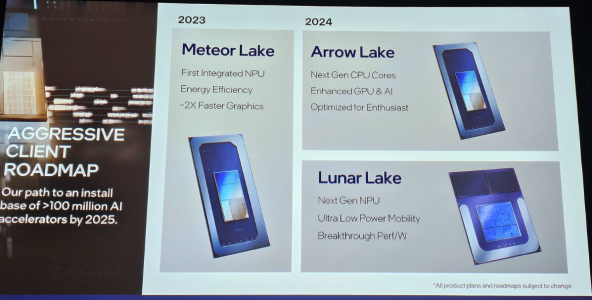
Possibly so; however, Higher overall performance is more important in most high profit markets. Where absolute performance ISN'T the biggest design constraint in the market, it is generally performance within a power envelope. I assume in your statement that you feel that Intel's Lunar Lake core is besting Zen 5 in the ultra light laptop market. AMD's design choices may be better suited to the data center where profits are much higher. Just a thought.
Since when is a 232mm2 die on N4P cheap?
Fair enough; however, one could argue that AMD should be using chiplets to avoid the yield issues and expense of the large monolithic die, but lets not be to clever by half here. Lunar Lake's compute tile alone is 140mm sq. It looks to be North of 200 mm sq total. Packaging is not free, nor is it free to produce the other 2 chips in the design.
For desktop and data center chips, AMD's design choices may look better. We will see soon enough.
That 80% market share in client means nothing for the orders from TSMC, and the entire Arrow Lake is now made of TSMC dies.
Intel is not getting pricing that is any better than AMD or Qualcomm. If anything, Intel's pricing is worse. Intel already announced it wants to shift production away from TSMC, so TSMC has zero incentive to offer Intel favorable pricing.
Given the fact that Arrow Lake is on N3B, for the CPU die while Zen 5 is N4P, Arrow Lake is on more expensive node and is also using more expensive packaging.
In short, no economies of scale, and cost disadvantage vs. Zen 5.
AMD likely has a disadvantage in the use of a single monolithic die in the mobile market (I am guessing yield, but certainly die per wafer) vs Lunar Lake compute tile; however, things may look quite different in the desktop and data center products (or even non "thin and light" laptop market that is 60-70% of the laptop market).