Intel "Haswell" Speculation thread

Page 24 - Seeking answers? Join the AnandTech community: where nearly half-a-million members share solutions and discuss the latest tech.

Nemesis 1

Lifer
Dec 30, 2006
11,366
2
0
How many people want a computer smaller than a Shuttle type, with one or no PCIe slots, limited panel IO (there's just not room!), and then having to rely mainly on USB for every non-special-function device added after the first two SATAs? OK, now of those people, how many of them are willing to pay more than a standard ATX case scenario, to get less system flexibility? A small percentage of Apple PC customers, and anyone buying a notebook/tablet/etc..
I am sure many would agree with ya on this as at this moment I do also . But its clear the trend is accelerating in the other direction . Because of space constraints in my water cooling rig and the need for Blue ray and more storage I went with Asus component encloser with blue ray . I also went that direction with the storage for music and video You also failed to mention Thunderbolt that is easily daisy chained the parts are a bit high right now but that will change in a year or 2 , Intel developed it at there cost and AMD is allowed to use it. this is the way forward
 
Last edited:

ShintaiDK

Lifer
Apr 22, 2012
20,378
145
106
Its been a process going on for quite a while.

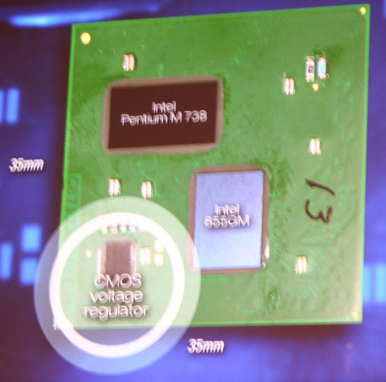
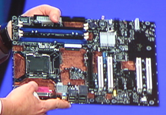
Lets try turn time back to 2005. Remember this? Haswell now reached that goal.

integratedGMCH.jpg

intelboard.jpg

Highlighted parts is whats removed with the integration.
 

Cerb

Elite Member
Aug 26, 2000
17,484
33
86
I am sure many would agree with ya on this as at this moment I do also . But its clear the trend is accelerating in the other direction . Because of space constraints in my water cooling rig and the need for Blue ray and more storage I went with Asus component encloser with blue ray . I also went that direction with the storage for music and video You also failed to mention Thunderbolt that is easily daisy chained
Daisy-chaining isn't what I meant. I was thinking of the need for an external video card or disk controller to need several connections in parallel to make it technically feasible to not use a slot on the board. Chaining and hubbing are cheap, but point-to-point (specifically, allowing for performance-critical devices to directly connect to an I/O hub that is close to the CPU and RAM, over an unshared connection) and parallelism are the ways performance trickles down [and out].

It can be done. It has been done, with video cards, even. It's just not cheap enough. As TB implementations get good enough in the future for current video, PCIe will leave it behind (isn't 32GB/s on x16 right around the corner, FI?).

There is definitely a trend downward, and it will continue. I will not build in a full-ATX case when I upgrade my desktop, FI. I'd rather save the space than have 3-4 more slots (I only need MicroATX because quiet video card coolers eat up 1-2 more slots!). But, the user flexibility offered by standards, like ATX, that necessitate much larger than technically necessarily boxes, and the bandwidth limitations of cheap external interfaces, are the main reason we still have them, instead of all using SFFs and AIOs.

The technology exists to allow >90% of PC users to conveniently have the Windows equivalent of an iMac, some with touch screens to boot (honestly, I kind of like the ones Gateway has been selling for several years, now). But they cost more, and they limit hardware upgrades over their lifetimes compared to normal sized, or even most cramped SFF, cases. Nettop-like teeny weeny integrated systems have the same issues as those stuffed into monitors, and have less room for case IO, too.
 
Last edited:

BenchPress

Senior member
Nov 8, 2011
392
0
0
Another question I have - would it be worth it to Intel to increase pipeline lengths a bit to maintain higher clocks (mainly for marketing) though with a higher branch misprediction penalty? Does Haswell improve on branch prediction or do anything to reduce the penalty? I read something about Haswell and branch prediction, but I can't find it (may have been speculation anyway).
First of all, it's not that simple. You can't increase the pipeline length by an arbitrary small amount. If you split one stage, you have to split many other stages or you end up having to make them do the same amount of work in less time, which costs area and/or power. So you quickly end up with lots of extra stages.

Secondly, there's really no need to increase the clocks for marketing reasons. People know about the MHz myth and the importance of IPC (but still have to learn about vector throughput). That said, I do believe there should be sufficient frequency headroom for the enthusiasts. Which is why I tried to come up with ways how they may have prevented sacrificing clock speed while adding a fourth ALU, and instead use the new process technology's characteristics to aggressively lower voltage and thereby power consumption. It's a whole other thing to expect increasing the clock frequency and taking a hit in branch misprediction penalty.

And lastly, branch prediction isn't something you can easily improve on demand. It suffers badly from diminishing returns. Even if you try to throw a lot of hardware at it, the predictor itself becomes slow. It's an uphill battle, and not the kind you want to be fighting in the first place.
 

IntelUser2000

Elite Member
Oct 14, 2003
8,686
3,785
136
I read something about Haswell and branch prediction, but I can't find it (may have been speculation anyway).

They state that branch prediction has been improved, but details have not been given.

Lets try turn time back to 2005. Remember this? Haswell now reached that goal.

Actually, Haswell has it on-die. They've exceeded that goal. :)
 

TuxDave

Lifer
Oct 8, 2002
10,572
3
71
Thanks fot that, very helpful :thumbsup:

Another question I have - would it be worth it to Intel to increase pipeline lengths a bit to maintain higher clocks (mainly for marketing) though with a higher branch misprediction penalty? Does Haswell improve on branch prediction or do anything to reduce the penalty? I read something about Haswell and branch prediction, but I can't find it (may have been speculation anyway).

I would kick marketing out of my cube if they wanted me to worsen a chip because it would "sound better"
 

NTMBK

Lifer
Nov 14, 2011
10,237
5,021
136
You also failed to mention Thunderbolt that is easily daisy chained the parts are a bit high right now but that will change in a year or 2 , Intel developed it at there cost and AMD is allowed to use it. this is the way forward

Thunderbolt offers the bandwidth of about a PCIe x4 socket. Tom's Hardware tried out external graphics over TB recently, and found that on anything faster than a GTX460 the TB link is a bottleneck: http://www.tomshardware.co.uk/pci-express-graphics-thunderbolt,review-32525.html Now combine that with other daisy chained devices eating up that bandwidth, and Thunderbolt just isn't a replacement for internal PCIe sockets. It's useful and serves a purpose- it gets fast IO and PCIe expansion into form factors where it just wasn't possible before, like tablets and ultrabooks. But it won't replace PCIe on the desktop, or the server.
 

Nemesis 1

Lifer
Dec 30, 2006
11,366
2
0
NTMBK thats not a reply of merit. Its nothing more than Red Herring argument. Were talking future not present. From your link .

There are many legitimate reasons to want an external chassis enabled with PCI Express slots. However, such a device would only be effective if it connected to a host machine over a high-speed interface. Thunderbolt is just that. Each link supports up to 10 Gb/s of bidirectional PCI Express-based throughput, or the equivalent of four second-gen lanes. That's enough bandwidth to do a lot of things, including gaming on a relatively high-end graphics card.

How long has Thunderbolt been around. 20GBs Total bandwidth for a first generation is pretty good . Intel says it will exceed 100Gbs in time more than enough. Hows USB compare to USB3?
It was Apple that made USB popular . It was apple that first used thunderbolt. AMD is allowed to use Thunderbolt yet they. going to push lighting bolt. What hardware company was it that actually did the real work on usb usb2 usb3? I come in here say a few things about what the future of hardware well look like and get were you getting this crap from . answer idf. IDF had a bit of meat to it this year . Something I really haven't seen talked about here is Radio . Not a whole lot written about it but radio is being ready to explode on the scene . Its a game changer . As we move forward the speed at which things advance is increaseing by 2x with every new problem solved. If man has a future its moving rapidly.
 

Ajay

Lifer
Jan 8, 2001
15,454
7,862
136
I would kick marketing out of my cube if they wanted me to worsen a chip because it would "sound better"

I've done that (not on a chip design), but the buggers still posted better numbers than I gave them. The magic that can be done if you really don't understand math ^_^
 

mrob27

Member
Aug 14, 2012
29
0
0
www.mrob.com
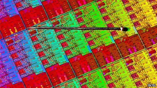
Take a look at this image:

_62821181_nail.jpg


Better yet, use Google Image Search to search for instances of this image on the web, and you'll find something very curious: This image only appears in a few articles about Haswell, the earliest of which was on Sep 11 2012.

The image is a typical publicity photo of the surface of a silicon wafer with the pattern of processor chips, with a pin lying on it to give a sense of scale. It is a common type of photo Intel releases when new products, such as IVB, SNB, NHM etc. are released.

I collect these photos every time they are released and I look at them closely. The chips in this wafer photo are different from all the others I've seen.

  1. There are clearly 4 CPU cores and a GPU, similar to the layout of 4-core IVB and SNB.
  2. The CPU cores are laid out differently, they look a bit like the left-hand-side cores of a SNB-E.
  3. The shader cores are positioned at the end (like IVB) not in a corner (like SNB),
  4. but there are 20 (or maybe 10) execution units: the wrong number for this to be a SNB or IVB, and the rest of the GPU area is laid out differently, too.

I believe this is a Haswell chip, but Intel only released it to the press briefly at the beginning of IDF and then changed their mind.
 

Idontcare

Elite Member
Oct 10, 1999
21,118
58
91
I believe this is a Haswell chip, but Intel only released it to the press briefly at the beginning of IDF and then changed their mind.

The aspect ratio of the die in your photo is 2.6:1

The aspect ratio of the die in the following known Haswell photo is 2.6:1

Intel-2012-Haswell-CPUs-Will-Feature-Improved-Multi-Core-Support-2_zps9d385bc9.jpg


Conclusion: I believe you to be correct, you have identified a die map of Haswell! :thumbsup:
 

NTMBK

Lifer
Nov 14, 2011
10,237
5,021
136
IDC, your aspect ratio comparison confuses me, because the die shot is quite obviously cropped...

The wafer shot is made up of multiple repeats of the same 2.6:1 segment. Each one of those segments is a Haswell die. Multiple chips are fabbed on a single wafer, then split up into separate chips.
 

Idontcare

Elite Member
Oct 10, 1999
21,118
58
91
IDC, your aspect ratio comparison confuses me, because the die shot is quite obviously cropped...

I don't follow you. Can you point out on the picture(s) what it is that is leaving you with the impression that the die shot is cropped?

By my count there are three fully uncropped die captured in the image mrob27 uploaded.
 

Charles Kozierok

Elite Member
May 14, 2012
6,762
1
0
IDC -- Never mind. I was confused and thought that was a partial picture of a single die, I can see now that there are several whole dice in the image. Sorry.. I blame it on the cold medicine. :)
 

Idontcare

Elite Member
Oct 10, 1999
21,118
58
91
IDC -- Never mind. I was confused and thought that was a partial picture of a single die, I can see now that there are several whole dice in the image. Sorry.. I blame it on the cold medicine. :)

Ah yes, I can see it now how the photo could be misinterpreted as each die being just one core (and thus we'd need four die to have an uncropped die image) rather than being 4 cores plus the GPU. Easy mixup, could happen to anyone.
 

Idontcare

Elite Member
Oct 10, 1999
21,118
58
91
So only question, what GT version is it :p

I'd say GT3 because the aspect ratio in the picture I linked is the same (2.6:1) and it is the one photo we have of Haswell on a PCB package that is an interposer package (note the unused landing pads above the die) which was expected to only be used with the GT3 variant of Haswell.
 

Ajay

Lifer
Jan 8, 2001
15,454
7,862
136
I'd say GT3 because the aspect ratio in the picture I linked is the same (2.6:1) and it is the one photo we have of Haswell on a PCB package that is an interposer package (note the unused landing pads above the die) which was expected to only be used with the GT3 variant of Haswell.

Thanks, I was scratching my head over what was up with all those extra "interconnects" - d'oh!
 

AtenRa

Lifer
Feb 2, 2009
14,001
3,357
136
I'd say GT3 because the aspect ratio in the picture I linked is the same (2.6:1) and it is the one photo we have of Haswell on a PCB package that is an interposer package (note the unused landing pads above the die) which was expected to only be used with the GT3 variant of Haswell.

Most definitely not GT3, i will say GT1 because the EU count is very low. GT3 suppose to have 40 EUs, GT3 should be close to half the die of a quad core Haswell.

Have a look at Intels HD4000 (IvyBridge) that has 16 EUs, the Shader area is larger than the picture in question. ;)


SandyBridge 12 EUs
sandybridgedieeus.jpg


IvyBridge 16 EUs
scaled.php


HasWell ???
hw2m.jpg


EDIT: Memory Controllers
Have a look at the memory controllers bellow the L3 Cache, the empty space is smaller than IvyBridge GT2 (HD4000) from the pic above, that only makes the die much smaller and thus not GT3 but probably GT1. ;)
 
Last edited:

Khato

Golden Member
Jul 15, 2001
1,206
250
136
Heh, here I thought it was pretty obvious via comparing to IVB GT2 that it's a picture of HSW GT2. The EU portion looks to basically be the exact same layout as IVB, just with 5 little 'yellow' dots instead of 4, therefore 20 EU instead of 16.
 

Ajay

Lifer
Jan 8, 2001
15,454
7,862
136
I started reading Here @ the RWT Forums


My first citation is Kanter's comments about various more complex theories regarding the additional ports added to Haswell:

Multi-cycle ALUs are bad
By: David Kanter (dkanter.delete@this.realworldtech.com), September 18, 2012 5:00 pm
Room: Moderated Discussions
Honestly, this theory is just silly:

1. Since the P4, Intel has avoided making changes which decrease performance of code. There are a ton of examples, including the FADD pipe on Haswell, and FADD is far less important than 64-bit ALU ops.

1a. Going to multi-cycle 64-bit ops would be a huge step backwards in performance and simply won't happen. Even IBM decided it was a horrible idea, and they own the platform. Intel has far less control over the SW ecosystem, making it an even worse idea.

1b. Software is already incorporating optimizations for Haswell, so if there were 2 cycle latency, it would be visible in this software.

2. Adding an integer/branch port is not a big deal.

2a. I have seen no evidence from you or anyone else that going from 7->8 ports impacts cycle time. It may not even be on the critical path at all.

2b. It only adds complexity to the integer forwarding network. Not SIMD or FP.

3. There is even less evidence that a 32-bit ALU would really improve cycle time relative to a 64-bit ALU. Moreover, Intel already has 64-bit ALUs that work fine on IVB - why would you think they are suddenly 'too slow' for Haswell? It makes no sense.

This 'theory' makes no sense and is entirely inconsistent with Intel's CPU design practices.

Anyway, you can continue arguing about it...but the answer is obvious to me.

David

Then Sevelto adds:

The SPCS001 slides contain more than enough answers

By: Gabriele Svelto (gabriele.svelto.delete@this.gmail.com), September 21, 2012 6:43 amRoom: Moderated Discussions
Nick (nicolas.capens.delete@this.gmail.com) on September 20, 2012 1:32 pm wrote:
> Are you suggesting to
> increase the delay between 0+6 and 1+5 instead? That actually doesn't complicate
> scheduling since the pairs take the same (integer) instruction types. The
> penalty might be incurred a little more frequently though.

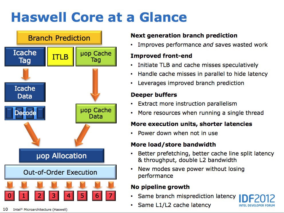
If you look at the slide deck for Haswell you'll see that it's highly unlikely that there have been increases the execution latencies, in fact the slides state the exact opposite. Check slide 10 for example:

http://www.theregister.co.uk/2012/09/20/intel_haswell_microarchitecture_deep_dive/page2.html

One of the bullet points reads: "More execution units, lower latencies"

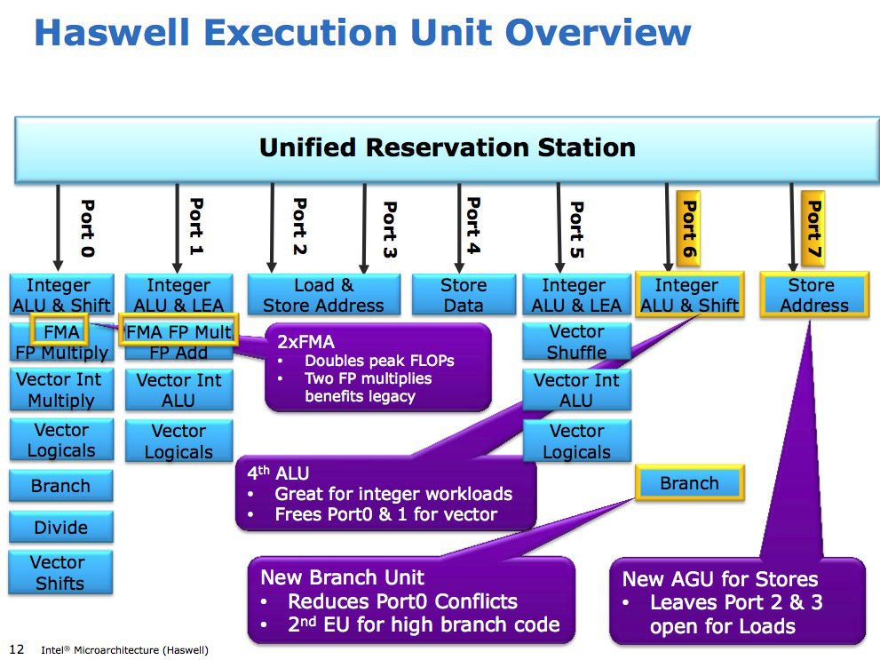
The rationale for the new ports on slide 12 is also pretty clear: the extra ports benefit both pure integer (cryptography mainly as Haswell is the only recent core not to feature extensive accelerators) and vector loads by relieving ports 0 & 1 from their double-duty of mixed issue.

As for the circuit design the changes seem very sensible, in spite of being an early 22nm design Ivy Bridge had significant headroom, Intel has likely into that headroom to provide increased performance at the same clocks. That is probably the best compromise between power and performance at this stage; that's even more sensible if you take into account that their high-end is unchallenged (and thus does not need any extra headroom) whilst their low-power offerings are being increasingly challenged in the mobile market.

Here's slide 12: (I know some, or all of these slides are on the AT Blog, but I hate the bottom to top inverse timeline - sorry Anand).

execution_unit_overview_large.jpg


And slide 10, which answers my question on pipeline length and some other questions I had:

haswell_computer_core_large.jpg


If someone here is actually Nicolas Capens, please note I mean no disrespect.

I wish RWT had nice forums like AT. Digging through them is a PITA!

One thing is clear to after reading many of these discussions, I'll have a heart attack if I ever need to understand the x86-64 ISA well enough to program @ the assembly level. No wonder AVX was under utilized. Now I'm almost rooting for ARM, so we eventually get some nice high powered RISC CPUs again in the mainstream** :thumbsup:

**I may go back to embedded development after completing my M.S.C.S. next year; fortunately most of that is still RISC based!
 

mrob27

Member
Aug 14, 2012
29
0
0
www.mrob.com
The aspect ratio of the die in your photo is 2.6:1

The aspect ratio of the die in the following known Haswell photo is 2.6:1

Intel-2012-Haswell-CPUs-Will-Feature-Improved-Multi-Core-Support-2_zps9d385bc9.jpg


Conclusion: I believe you to be correct, you have identified a die map of Haswell! :thumbsup:

I thought of that, but we already know that there are four distinct Ivy Bridge dies and the leaks suggest that there will be at least as many Haswells.

So we can't be sure that this recent photo shows the same chip as that 2011 IDF photo or the early QS sample photos (formerly here. Sure, it's plausible, but not enough to convince me.
 
Last edited:

mrob27

Member
Aug 14, 2012
29
0
0
www.mrob.com
Most definitely not GT3, i will say GT1 because the EU count is very low. GT3 suppose to have 40 EUs, GT3 should be close to half the die of a quad core Haswell.

Have a look at Intels HD4000 (IvyBridge) that has 16 EUs, the Shader area is larger than the picture in question. ;)


SandyBridge 12 EUs (image is here)

IvyBridge 16 EUs(image is here)

HasWell ???
hw2m.jpg


EDIT: Memory Controllers
Have a look at the memory controllers bellow the L3 Cache, the empty space is smaller than IvyBridge GT2 (HD4000) from the pic above, that only makes the die much smaller and thus not GT3 but probably GT1. ;)

Yep. My guess is that this is a 20-EU Haswell, i.e. a GT2. The only hints I have seen about the GT3 layout indicate that it will be a sort of square die (from the 128M L4 cache rumor, VR-Zone, 2012 March 18) :

dieimage.jpg