Intel 10nm and GF 7nm at IEDM 2017

raghu78

Diamond Member
Aug 23, 2012
4,093
1,475
136
(Paper 29.1, “A 10nm High Performance and Low-Power CMOS Technology Featuring 3rd-Generation FinFET Transistors, Self-Aligned Quad Patterning, Contact Over Active Gate and Cobalt Local Interconnects,” C. Auth et al, Intel)

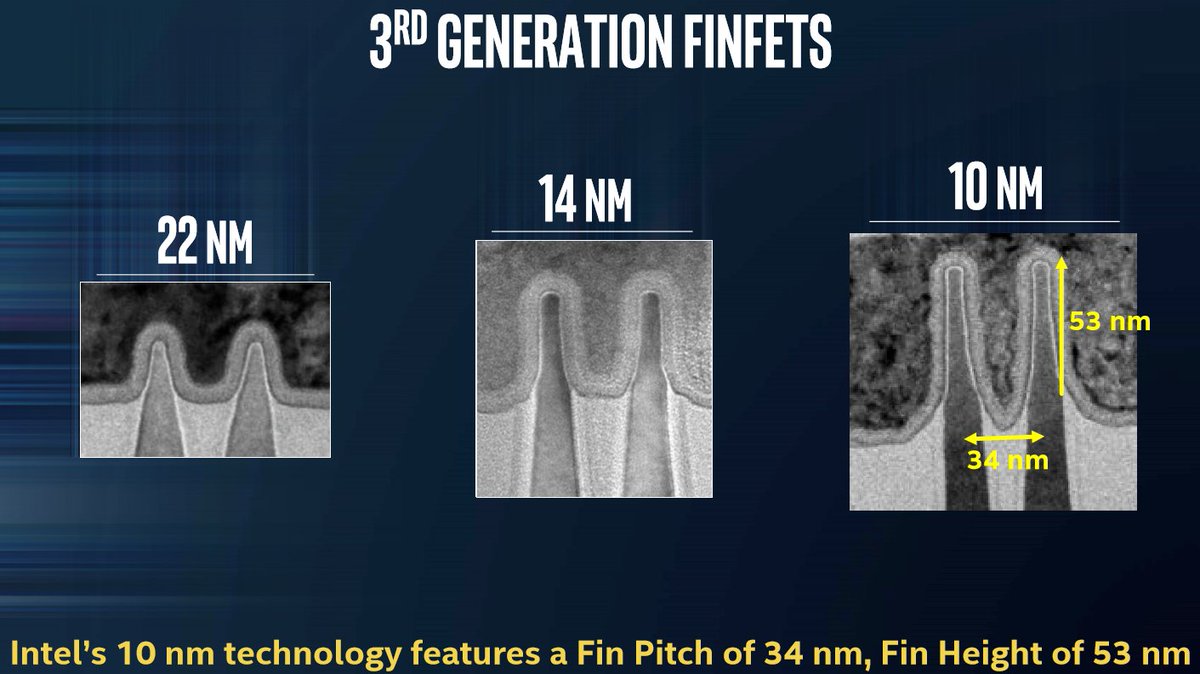
Intel researchers will present a 10nm logic technology platform with excellent transistor and interconnect performance and aggressive design-rule scaling. They demonstrated its versatility by building a 204Mb SRAM having three different types of memory cells: a high-density 0.0312µm2 cell, a low voltage 0.0367µm2 cell, and a high-performance 0.0441µm2 cell. The platform features 3rd-generation FinFETs fabricated with self-aligned quadruple patterning (SAQP) for critical layers, leading to a 7nm fin width at a 34nm pitch, and a 46nm fin height; a 5th-generation high-k metal gate; and 7th-generation strained silicon. There are 12 metal layers of interconnect, with cobalt wires in the lowest two layers that yield a 5-10x improvement in electromigration and a 2x reduction in via resistance. NMOS and PMOS current is 71% and 35% greater, respectively, compared to 14nm FinFET transistors. Metal stacks with four or six workfunctions enable operation at different threshold voltages, and novel self-aligned gate contacts over active gates are employed.


29-1%20Auth_Fig%2013.jpg


You can find the press kit at http://btbmarketing.com/iedm/
 

raghu78

Diamond Member
Aug 23, 2012
4,093
1,475
136
(Paper 29.5, “A 7nm CMOS Technology Platform for Mobile and High-Performance Compute Applications,” S. Narasimha et al, Globalfoundries)

Globalfoundries researchers will present a fully integrated 7nm CMOS platform that provides significant density scaling and performance improvements over 14nm. It features a 3rd-generation FinFET architecture with self-aligned quadruple patterning (SAQP) used for fin formation, and self-aligned double patterning for metallization. The 7nm platform features an improvement of 2.8x in routed logic density, along with impressive performance/power responses versus 14nm: a >40% performance increase at a fixed power, or alternatively a power reduction of >55% at a fixed frequency. The researchers demonstrated the platform by using it to build an incredibly small 0.0269µm2 SRAM cell. Multiple Cu/low-k BEOL stacks are possible for a range of system-on-chip (SoC) applications, and a unique multi-workfunction process makes possible a range of threshold voltages for diverse applications. A complete set of foundation and complex IP (intellectual property) is available in this advanced CMOS platform for both high-performance computing and mobile applications.

29-5%20Narasimha_Fig%202.jpg


29-5%20Narasimha_Fig%2014.jpg


CatMerc

Golden Member
Jul 16, 2016
1,114
1,149
136
Holy hell the curve on that 7nm HPC. That's probably something only IBM will use.

7nm SoC looks pretty damn promising for Zen2's frequency.

Edit: Can these be mixed and matched within a single chip? Like using 7nm HPC on critical paths and then giving 7nm SoC to the rest.
 
Last edited:

IntelUser2000

Elite Member
Oct 14, 2003
8,686
3,785
136
Intel claims each of the + generations for 14nm brings only 10-12% increase in drive current. Cumulatively, 14nm++ is only 20-25% higher in drive current compared to the original 14nm process.

With 10nm they are claiming 35-70% increase in drive current over original 14nm process. Are they measuring something different from 14nm data? Perhaps 14nm is at 1V, while 10nm comparisons are at 0.7V?

They claim even 10nm+ doesn't beat 14nm++. This data doesn't correlate with that.
 
  • Like
Reactions: ajc9988

raghu78

Diamond Member
Aug 23, 2012
4,093
1,475
136
Holy hell the curve on that 7nm HPC. That's probably something only IBM will use.

7nm SoC looks pretty damn promising for Zen2's frequency.

Edit: Can these be mixed and matched within a single chip? Like using 7nm HPC on critical paths and then giving 7nm SoC to the rest.

Yes you are right. From the freq/power graph we can roughly estimate 7 HPC brings 30% higher frequency over 7 SoC but at 2.5x the power. My guess is Zen 2 for desktop will use 7 HPC as they would want 4.5+ Ghz max clocks. AMD could use 7SoC for Zen 2 server chips as those are unlikely to need more than 3.5 Ghz turbo. GF stated that 7LP will be good for ARM A72 designs clocked at 3.5 Ghz.

http://www.eenewseurope.com/news/gf-debuts-7nm/page/0/1

"The process is geared for the same kinds of premium cloud and smartphone processors as today’s 14/16nm nodes. An ARM Cortex-A72 core could run at more than 3.5 GHz in the process, the company estimates."

About mixing 7HPC and 7SoC on the same chip thats something only AMD chip designers or a process/chip design expert can comment on.

Intel claims each of the + generations for 14nm brings only 10-12% increase in drive current. Cumulatively, 14nm++ is only 20-25% higher in drive current compared to the original 14nm process.

With 10nm they are claiming 35-70% increase in drive current over original 14nm process. Are they measuring something different from 14nm data? Perhaps 14nm is at 1V, while 10nm comparisons are at 0.7V?

They claim even 10nm+ doesn't beat 14nm++. This data doesn't correlate with that.

Intel is probably making comparisons for low power chips given that Cannonlake is launching in low power ultrathins and tablets only. The first 10nm desktop chip is Icelake. Intel 14nm and 22nm where less impressive against their foundry counterparts (28nm and 16/14nm) in the low power space but for high performance 14+/14++ are the best in the semiconductor industry.
 

CatMerc

Golden Member
Jul 16, 2016
1,114
1,149
136
Yes you are right. From the freq/power graph we can roughly estimate 7 HPC brings 30% higher frequency over 7 SoC but at 2.5x the power. My guess is Zen 2 for desktop will use 7 HPC as they would want 4.5+ Ghz max clocks. AMD could use 7SoC for Zen 2 server chips as those are unlikely to need more than 3.5 Ghz turbo. GF stated that 7LP will be good for ARM A72 designs clocked at 3.5 Ghz.

http://www.eenewseurope.com/news/gf-debuts-7nm/page/0/1

"The process is geared for the same kinds of premium cloud and smartphone processors as today’s 14/16nm nodes. An ARM Cortex-A72 core could run at more than 3.5 GHz in the process, the company estimates."

About mixing 7HPC and 7SoC on the same chip thats something only AMD chip designers or a process/chip design expert can comment on.


Intel is probably making comparisons for low power chips given that Cannonlake is launching in low power ultrathins and tablets only. The first 10nm desktop chip is Icelake. Intel 14nm and 22nm where less impressive against their foundry counterparts (28nm and 16/14nm) in the low power space but for high performance 14+/14++ are the best in the semiconductor industry.
AMD isn't likely to create two very similar chips with the only difference being variants of a process. Zen 2 will either be SoC or HPC, and I'm leaning on SoC for server's sake. Clockspeeds over 14nm should still be a major leap, with theoretically 4.4GHz at the same power as Zen currently does 3.2GHz. So basically a 1700 power consumption wise + 1.4GHz. And clock ceiling should increase too. Taking the chart literally (which is dangerous but roll with it), it would be around 5.3GHz ceiling.

Question still remains about mixing HPC and SoC in a single chip. That could provide a best of both worlds type of deal.
 

raghu78

Diamond Member
Aug 23, 2012
4,093
1,475
136
AMD isn't likely to create two very similar chips with the only difference being variants of a process. Zen 2 will either be SoC or HPC, and I'm leaning on SoC for server's sake. Clockspeeds over 14nm should still be a major leap, with theoretically 4.4GHz at the same power as Zen currently does 3.2GHz. So basically a 1700 power consumption wise + 1.4GHz. And clock ceiling should increase too. Taking the chart literally (which is dangerous but roll with it), it would be around 5.3GHz ceiling.

Question still remains about mixing HPC and SoC in a single chip. That could provide a best of both worlds type of deal.

I do not see 7HPC being used for Zen 2 server given the freq/power curve is so much better for 7SoC. But having said that using 7SoC for desktop means Zen 2 cannot hit 4.5+ Ghz which I think is a serious compromise if AMD want to compete with Intel for ST and gaming performance. In fact I think the sweet spot for 7SoC is probably 3.3-3.5 Ghz which is where most ARM SoCs will clock.
 
Mar 10, 2006
11,715
2,012
126
With 10nm they are claiming 35-70% increase in drive current over original 14nm process. Are they measuring something different from 14nm data? Perhaps 14nm is at 1V, while 10nm comparisons are at 0.7V?

They would not compare drive currents at different voltages; these comparisons have always been at the same voltage in previous papers.
 
  • Like
Reactions: lightmanek

Abwx

Lifer
Apr 2, 2011
10,854
3,298
136
I do not see 7HPC being used for Zen 2 server given the freq/power curve is so much better for 7SoC. But having said that using 7SoC for desktop means Zen 2 cannot hit 4.5+ Ghz which I think is a serious compromise if AMD want to compete with Intel for ST and gaming performance. In fact I think the sweet spot for 7SoC is probably 3.3-3.5 Ghz which is where most ARM SoCs will clock.

The graph show 7nm SOC hitting 30% higher Fmax than 14nm, at about 80% of the power.
 

Tuna-Fish

Golden Member
Mar 4, 2011
1,324
1,462
136
Edit: Can these be mixed and matched within a single chip? Like using 7nm HPC on critical paths and then giving 7nm SoC to the rest.

No.

If AMD wanted to make chips on 7nm HPC, one option they'd have is to make EPYC/TR style chips where they have multiple dies, one of which is designed for higher power consumption and clocks.

I don't think this is likely, though, as the 7nm HPC process requires different masks, and mask sets are expensive these days.

About mixing 7HPC and 7SoC on the same chip thats something only AMD chip designers or a process/chip design expert can comment on.

No, it's something anyone with any knowledge of how these things are built can tell you. If it was possible for these to coexist on a single chip, they would not be marketed as separate processes, they would just be different logic elements that are available as a part of a single process.

(And the reason they cannot coexist, if anyone is interested: When making chips, the only operation that provides precision in the vertical dimension is polishing. That is, to add a specific height of (for example) dielectric, they cannot just add x amount, they have to first add quite a bit more than they want, and then polish out the excess, smoothing out the entire chip to that height. This means that they have to build all transistors on the chip at the same time, and that they need to have the same vertical dimensions. If they tried to build two different kinds of transistors with different vertical height, they would be destroying the ones they built first when they went on to build the second set.)
 

jpiniero

Lifer
Oct 1, 2010
14,511
5,159
136
Hmm, GloFo is also using SAQP for the first gen 7 nm. I am thinking that is Intel's biggest problem with 10 nm... If GloFo manages to produce 7 nm at sellable yield only a couple months after Intel gets to that point that is pretty embarrassing for Intel.
 

raghu78

Diamond Member
Aug 23, 2012
4,093
1,475
136
Hmm, GloFo is also using SAQP for the first gen 7 nm. I am thinking that is Intel's biggest problem with 10 nm... If GloFo manages to produce 7 nm at sellable yield only a couple months after Intel gets to that point that is pretty embarrassing for Intel.

GF is using SAQP for only the transistor fins and SADP for metal layers while Intel is using SAQP for both the transistor fins and the lowest metal layers as Intel 10nm Minimum metal picth is 36nm while GF 7nm Minimum metal pitch is 40nm. SADP limit is 40nm.

https://www.semiwiki.com/forum/content/6498-2017-leading-edge-semiconductor-landscape.html
 
  • Like
Reactions: lightmanek
Mar 10, 2006
11,715
2,012
126
Hmm, GloFo is also using SAQP for the first gen 7 nm. I am thinking that is Intel's biggest problem with 10 nm... If GloFo manages to produce 7 nm at sellable yield only a couple months after Intel gets to that point that is pretty embarrassing for Intel.

TSMC is already using quad patterning to pattern the fins on its 10nm technology (fin pitch of 36nm).

TSMC 10 nm was found in the Apple A10X processor (APL1071) found in the Apple iPad Pro 10.5 (MQDT2CL/A). Taking a deeper look inside the TSMC 10 nm, our experts found quad-patterned FinFETs, which are first in the industry.

http://techinsights.com/technology-intelligence/overview/latest-reports/tsmc-10-nm-process/
 
  • Like
Reactions: ksec

Excessi0n

Member
Jul 25, 2014
140
36
101
Holy hell the curve on that 7nm HPC. That's probably something only IBM will use.

Doesn't look that bad. The low end of the HPC curve is the same power as the high end of the 14nm curve but with much higher frequency. Using a lot of power isn't a problem if you've got the clocks to back it up. And there are plenty of areas where performance per watt isn't the chief concern, anyways.

Admittedly, I might be rationalizing because I really want an AMD chip which will overclock to the moon. My body loop is ready.
 
Last edited:

CatMerc

Golden Member
Jul 16, 2016
1,114
1,149
136
Doesn't look that bad. The low end of the HPC curve is the same power as the high end of the 14nm curve but with much higher frequency. Using a lot of power isn't a problem if you've got the clocks to back it up. And there are plenty of areas where performance per watt isn't the chief concern, anyways.

Admittedly, I might be rationalizing because I really want an AMD chip which will overclock to the moon. My body loop is ready.
Efficiency advanacements are important for the most lucrative server market. 7nm SoC is the best for that.

The only place 7nm HPC is more efficient on that graph is when 14nm is at the top of the curve (least efficient), and the HPC process is at the bottom of the curve (most efficient).
Meanwhile at every single point on the graph 7nm SoC is more efficient.

Unless AMD is going to create two different dies, one for servers and one for desktops (which goes against all that they've done recently), Zen 2 will be 7nm SoC based.
 
Last edited:

krumme

Diamond Member
Oct 9, 2009
5,952
1,585
136
Efficiency advanacements are important for the most lucrative server market. 7nm SoC is the best for that.

The only place 7nm HPC is more efficient on that graph is when 14nm is at the top of the curve (least efficient), and the HPC process is at the bottom of the curve (most efficient).
Meanwhile at every single point on the graph 7nm SoC is more efficient.

Unless AMD is going to create two different dies, one for servers and one for desktops (which goes against all that they've done recently), Zen 2 will be 7nm SoC based.
I tend to agree. But look at it this way:
Right now they have 2 dies covering near the entire market. Both 14llp one 4c one 8c from the same ccx. It perfect for servers and mobile.
Now i am sure they will do that again. Efficiency is king here.

But can desktop meaning gaming and to some degree a few professional apps pay for a very high fmax die from the same used for servers?

I am not sure its out of the question because 25% fmax uplift can imo easily get you 60% for the same number of cores if it tilts you over your competitor. Premium perf attracts huge margins. It is seldom logic but more feelings and brand.
Amd is pretty bad at that sort of thinking so i dont hink they go there but off the bat looking at those curves i would do it any time of the week.
When you have easy access to that sort of high fmax process via ibm and the synergy to the brand value is huge even if the start cost is 200M i would go there. Amd need too start doing stuff like that. That is if the curves is true and gives them the compettitive edge.
 

el etro

Golden Member
Jul 21, 2013
1,581
14
81
And that gives 4.95Ghz at less than 95Watts, 8-core.

My bad. According to the Graph, Ryzen7 1800x may clock at 4.7Ghz base and 5.2Ghz 1-core turbo clock. All-core turbo can be 4.8Ghz.
This at 7nm SoC version.
 

Yotsugi

Golden Member
Oct 16, 2017
1,029
487
106
Sounds like GloFo manages to offer higher density than Intel.
Duh, IBM infusion surely is nice.
My bad. According to the Graph, Ryzen7 1800x may clock at 4.7Ghz base and 5.2Ghz 1-core turbo clock. All-core turbo can be 4.8Ghz.
This at 7nm SoC version.
Sounds pretty nice.
I wonder what kind of performance 10++ will deliver and if it's ever going to be competitive against 7LP with EUV.