History of Intel Graphics cards
yjfy
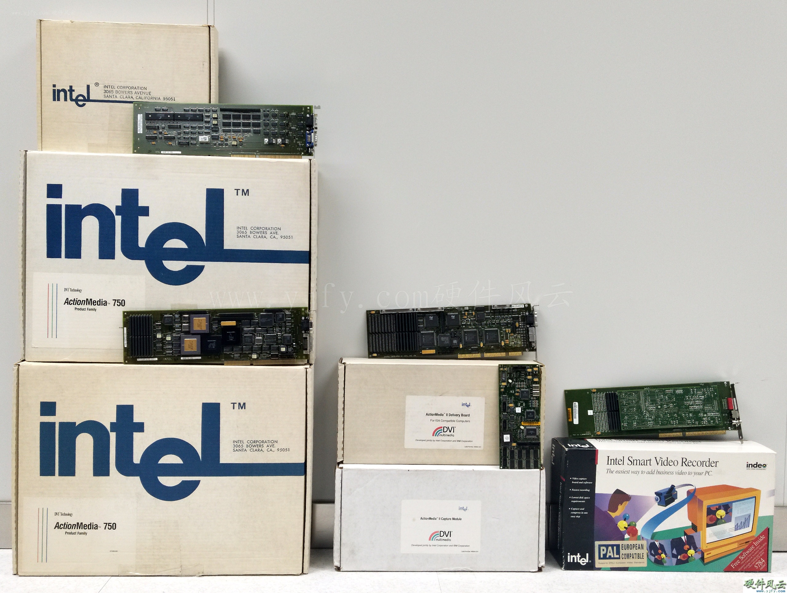
This article is about the history of Intel's graphics and display chips based on hardware collections. In order to reflect the authority of this article, the intel graphics cards in the text are mostly representative engineering samples from myself and Tibetan friends. Thanks to the computer hardware collection, such rare computer hardware can get rid of destruction.
This article introduces the history of Intel graphics cards into four periods.
1. 12 years of drifting ( 1977-1988 )
Intel's original graphics card is for VIDEO/GRAPHICS MODULE on Intel Single Board Computers, a display module with display capabilities. Although it is only the prototype of the graphics card, it has an important position in the history of Intel graphics. After Intel released several display chips, it was used by many manufacturers to make graphics cards, but Intel still disdain to enter the PC graphics market, because Intel's business focus at this time is memory and processor.
1.1 8275 Chip
yjfy
This article is about the history of Intel's graphics and display chips based on hardware collections. In order to reflect the authority of this article, the intel graphics cards in the text are mostly representative engineering samples from myself and Tibetan friends. Thanks to the computer hardware collection, such rare computer hardware can get rid of destruction.
This article introduces the history of Intel graphics cards into four periods.
1. 12 years of drifting ( 1977-1988 )
Intel's original graphics card is for VIDEO/GRAPHICS MODULE on Intel Single Board Computers, a display module with display capabilities. Although it is only the prototype of the graphics card, it has an important position in the history of Intel graphics. After Intel released several display chips, it was used by many manufacturers to make graphics cards, but Intel still disdain to enter the PC graphics market, because Intel's business focus at this time is memory and processor.
1.1 8275 Chip
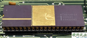
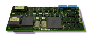
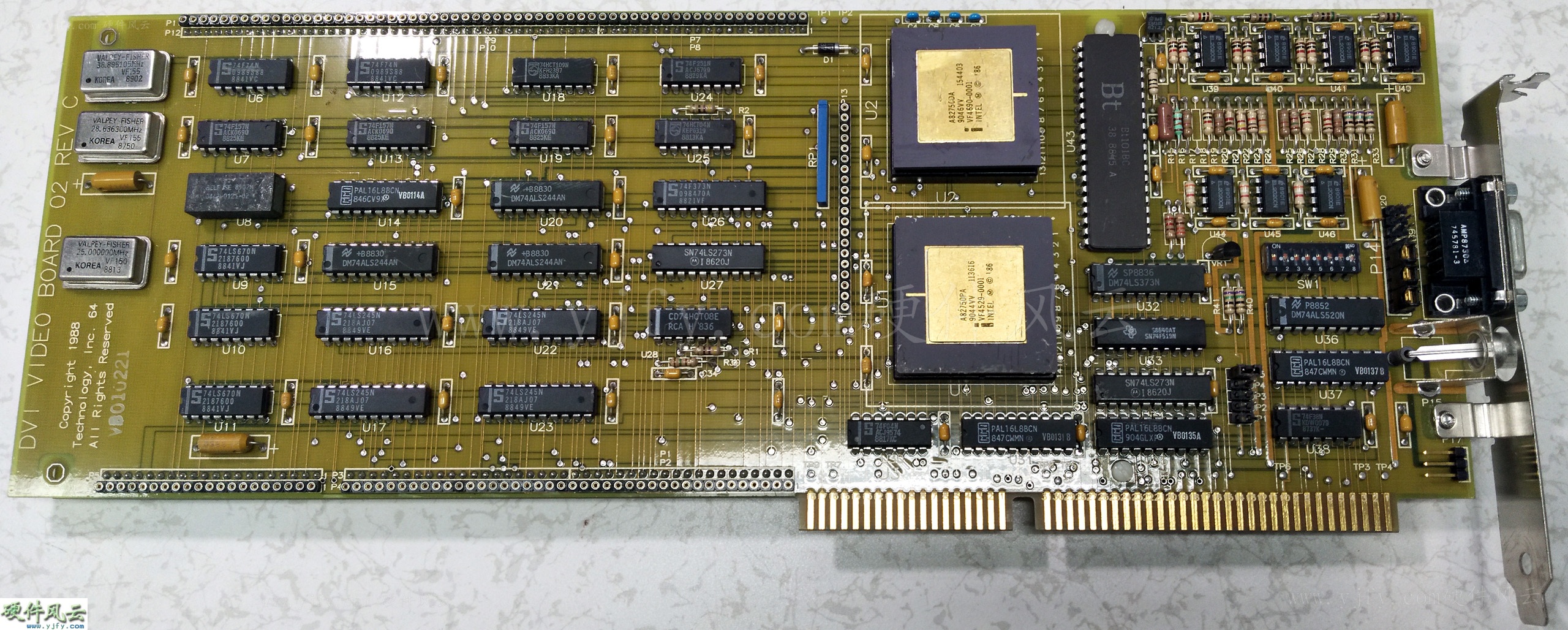
C8275 Engineering sample
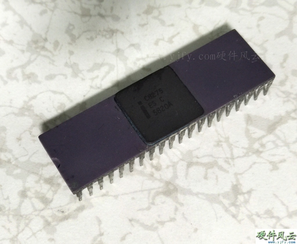
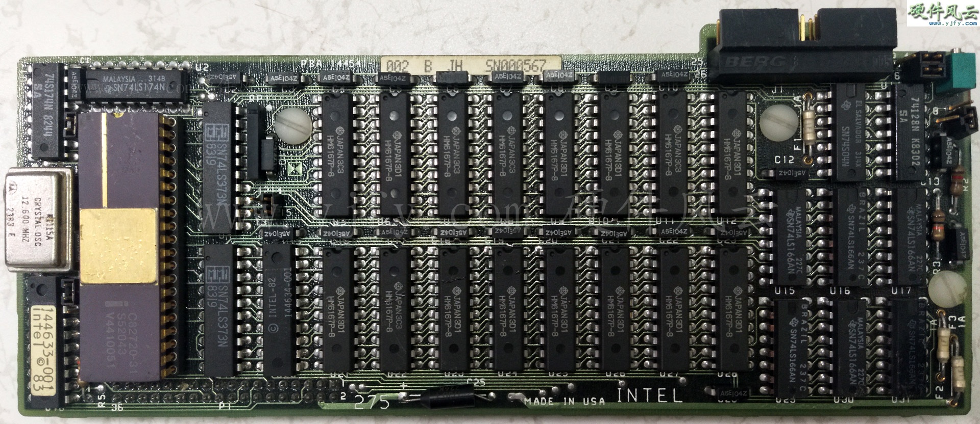
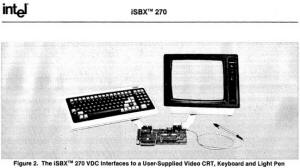
Pictured above is Intel's first display-related chip C8275 CRT Controller, which is an engineering sample chip with a date of 7735, indicating that the C8275 chip first appeared in the 35th week of 77 (late mid-August). Used in Intel's iSBX270 VIDEO DISPLAY CONTROLLER MULTIMODULE Board. The iSBX 270 VDC contains 4K bytes of high speed static RAM.
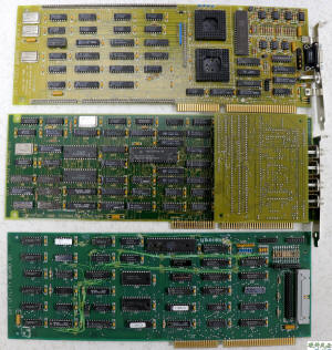
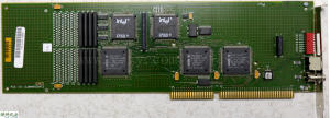
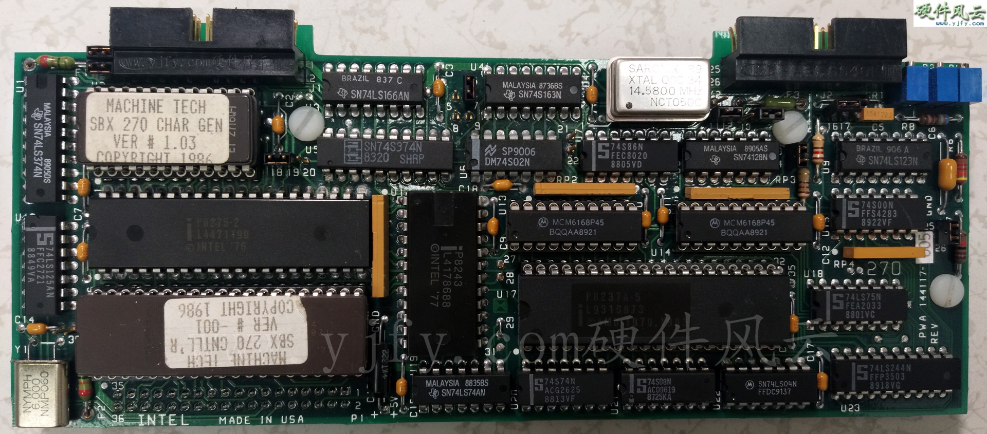
iSBX270
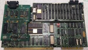
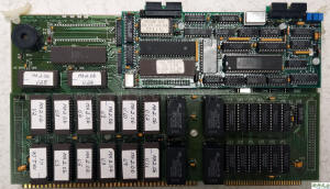
Processor II 2217605132
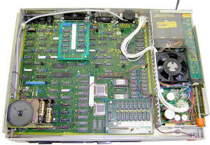
The iSBX270 was well-known in the past and was also used on the Processor II 2217605132 Multibus card from non-intel Machine Technology Inc.
Processor II 2217605132
Last edited: