
- Sep 5, 2003
- 19,458
- 765
- 126
Nvidia is announcing two products today, two Kepler based HPC / GPGPU cards - K10 and K20.
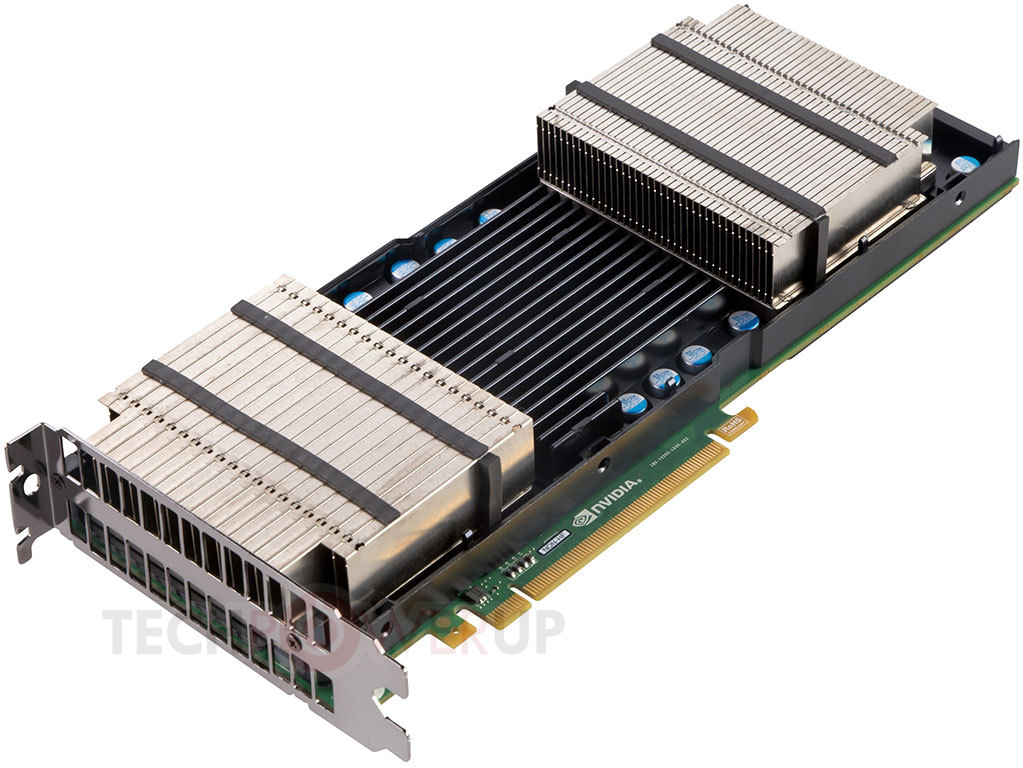
NVIDIA Tesla K10
Tesla K10 dedicated to seismic analysis where most valuable resource is bandwidth. It has 3x single precision of todays fermi tesla and 1.8x the memory bandwidth.
NVIDIA is preparing two Tesla GPUs, one is Tesla K10, based on dual-GK104 chips, which is to be devoted to high efficient computing in oil and gas exploration and defense industry. Card is based on dual-GK104 GPUs and has a memory bandwidth of 320 GB/s.
The Tesla K10 packs two Kepler-based GK104 GPUs and 8 GBs of VRAM.
Source
This is basically a GTX690 with 4GB of VRAM per GPU.
NVIDIA Tesla K20
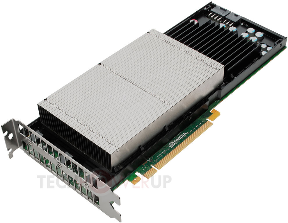

Second Tesla, K20 is focused on double precision: 3x double precision of fermi, includes hyper q, dynamics parallelism, for stuff like physics, quantum chemistry, computational finance.
GK110: Actual chip is to feature 15 SMXs (streaming multiprocessors) with 192 CUDA cores each. This gives 2,880 CUDA cores in total.
GK110 GPU which is coming in Q4 of this year.
Source
Update: GK110 2-page PDF
GTC Live feeds - Click Here.
Update #2: NVIDIA disclosed that the Tesla K10 offers a memory bandwidth as high as 320 GB/s. - TechPowerup
Thoughts: It is now official -- GK104 is not the high-end Kepler chip. It just happens to be the high-end gaming chip at the moment. Looks like NV is pushing for higher profit margins by selling GK110 in the professional markets. I think GK110 will become GTX780 and launch in 2013 at this point.
Update #3: Rumored Specs for GK110
Full physical GK110
15 SMX @ 192 CUDA Cores = 2,880 SPs
K20 Tesla parts will likely have 13-14 of SMX clusters enabled = 2,496 - 2,688 SPs
384-bit memory bus
TDP > 225W
K20 Tesla Launch Date: Q4 2012
Consumer GK110 Launch Date: 2013
Source 1
Source 2
Thanks to Sontin and Cookie Monster for finding that info and breaking it down.
NVIDIA Tesla K10
Tesla K10 dedicated to seismic analysis where most valuable resource is bandwidth. It has 3x single precision of todays fermi tesla and 1.8x the memory bandwidth.
NVIDIA is preparing two Tesla GPUs, one is Tesla K10, based on dual-GK104 chips, which is to be devoted to high efficient computing in oil and gas exploration and defense industry. Card is based on dual-GK104 GPUs and has a memory bandwidth of 320 GB/s.
The Tesla K10 packs two Kepler-based GK104 GPUs and 8 GBs of VRAM.
Source
This is basically a GTX690 with 4GB of VRAM per GPU.
NVIDIA Tesla K20
Second Tesla, K20 is focused on double precision: 3x double precision of fermi, includes hyper q, dynamics parallelism, for stuff like physics, quantum chemistry, computational finance.
GK110: Actual chip is to feature 15 SMXs (streaming multiprocessors) with 192 CUDA cores each. This gives 2,880 CUDA cores in total.
GK110 GPU which is coming in Q4 of this year.
Source
Update: GK110 2-page PDF
GTC Live feeds - Click Here.
Update #2: NVIDIA disclosed that the Tesla K10 offers a memory bandwidth as high as 320 GB/s. - TechPowerup
Thoughts: It is now official -- GK104 is not the high-end Kepler chip. It just happens to be the high-end gaming chip at the moment. Looks like NV is pushing for higher profit margins by selling GK110 in the professional markets. I think GK110 will become GTX780 and launch in 2013 at this point.
Update #3: Rumored Specs for GK110
Full physical GK110
15 SMX @ 192 CUDA Cores = 2,880 SPs
K20 Tesla parts will likely have 13-14 of SMX clusters enabled = 2,496 - 2,688 SPs
384-bit memory bus
TDP > 225W
K20 Tesla Launch Date: Q4 2012
Consumer GK110 Launch Date: 2013
Source 1
Source 2
Thanks to Sontin and Cookie Monster for finding that info and breaking it down.
Last edited:

