ShintaiDK
Lifer
- Apr 22, 2012
- 20,378
- 146
- 106
Of course. Which leads to the funny situation, that higher CB scores are touted as higher IPC, while with going from 128b to 256b SIMD the IPC actually went down.")
Cinebench doesnt use 256bit SIMD.

Of course. Which leads to the funny situation, that higher CB scores are touted as higher IPC, while with going from 128b to 256b SIMD the IPC actually went down.
For single threaded IPC, 40% over Excavator is about 0.5% over Haswell.
It should beat an i5 easily (AMD usually doesn't do much differentiation based on enabled features, so I expect all of their CPUs will have SMT enabled - except, maybe, Athlons and Semprons when/if those arrive with Zen cores).
The real chore for Zen is to match or beat the Haswell i7s in single threaded, and maybe catch up with Skylake in multithreaded loads (AMD's usually scale better than Intel, and if Zen's data fabric and cache layout are as claimed, this should be no exception).
That comes down to its SMT, though, or willingness to throw more cores into the fray. I'd be very surprised if AMD's SMT was equal to Intel's SMT, but they have probably learned a great deal from the CMT design and may well have kept many elements of Bulldozer's front-end to leverage for SMT. With the instructions being fed and retired single-file they would lose most of the module-induced pipeline stages, so I'd expect a 14~17 cycle pipeline on Zen, much like Sandy Bridge.
BTW, what is the base of the 40% increase? Average, lowest, or highest XV IPC in many or some benchmarks? Or SPEC CPU as usual?
Doing two 256b AVX ops per cycle vs. 128b doesn't increase IPC (technically).
Hopefully the design doesn't require SMT to be at play to realize that 40% boost. If so, single threaded performance could see a mere 10% or so boost... but, we'd get that just from dropping the module pipeline overhead... and we'd get more still from going with wider cores... So it would only make sense that AMD was aiming at a true 40% per core, single threaded, per cycle improvement.
On the FPU front, with AMD, doubling the FPU, itself, allows more operations to be executed at once.
It's really all about the addressable execution units, rather than an "FPU." Bulldozer's FPU is said to be 128x2, but is, in reality, 4x64 FMAC + 4x64 FADD...
Think about it differently, one EXV core manage to use the FPU at 60% only, the two cores manage to max it at close to 100%, there s no need to double the FPU to extract more FP throughput out of a single core.
What must be doubled is the ALU + AGLU count, FP ops are managed by the (ALUs + AGLUs) since these latters control the load store unit and check the completion of the processed operations, the FPU is just the unit that execute the mathematical computation.
As for the FPU width it s 4 64bits units but they can be used simultaneously, indeed there s no 128bit unit that exist in any CPU, these are exclusively 64bits units, when there s two such units and that they can execute each one operation/cycle using a single instruction then it is called 128bit, wich is somewhat not accurate technicaly speaking.
Sure, this is some of the module overhead of which I speak. AMD could see a decent floating point boost without doing anything other than divorcing the unit from the module. But I doubt they will stop at that, it wouldn't get them anywhere in the server world unless they could seriously reduce power usage to well below Intel's.
I don't think FPU performance has been bound by AL[G]U performance with AMD since either the K8 or K10. The FPU has its own scheduler directly from the dispatcher, after decoding. The FPU has been an AMD strong point for some time, only the module design hinders its true performance from being revealed.
Yeah, it's not all about the operand and execution unit sizes. K10, IIRC, could perform a max of two FLOPs/cycle since it couldn't pull in any more information at once. Bulldozer has a higher limit, but I can't remember what it was, but I don't think they could fully flood the FPU without SIMD.

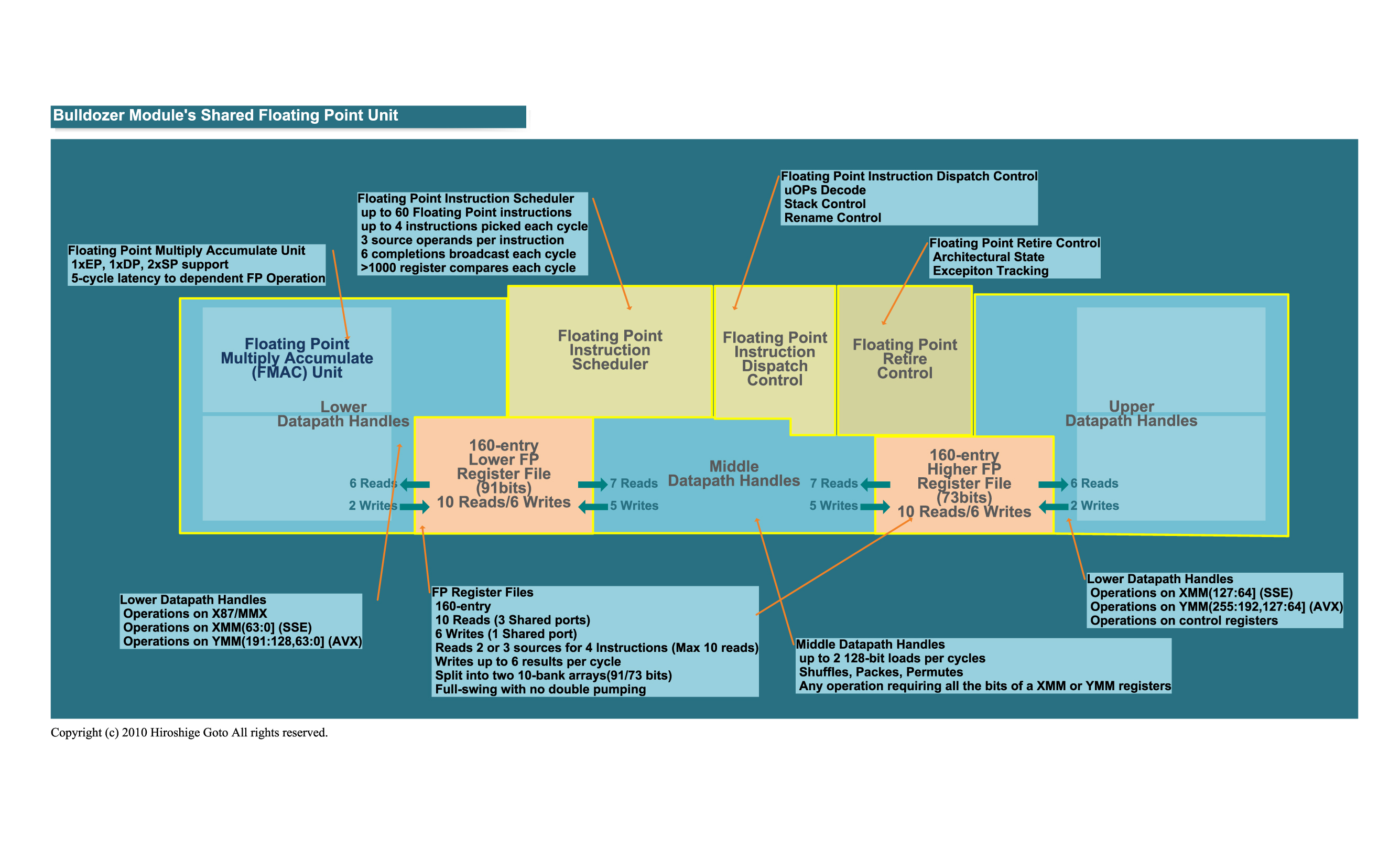
Scheduler does only a small part of the work as a X86 instruction imply several uops, in the diagram below we can see that each core has its own L/S unit, as said the operands and operation that are used by the FPU are managed by the thead parent core and maths operations completion is done by the ALU + AGU.
thumbsdown:Just a warning: Whoever put my speculative uarch schematic with added colors on Wikipedia, didn't correct my early wrong assumption about the FP units' functionalities. It's been there for years already.
There are NDAs to cover possible leaks. But as I know a long time GF'er (working there since first Fab 30 production), I know that at that stage there isn't much to know about the microarchitecture, but more about power and frequency. So it likely happens at many design levels. And ASMedia just needs to know the interfaces, nothing more.
14nm production should be covered by AMD as they integrate the ASMedia stuff. The latter might get the design rules and tooling, but don't need to create their own chips. As you've seen the last years, there are final product designs already with the second stepping. Mask set prices drove pre-production testing efforts.
Just a warning: Whoever put my speculative uarch schematic with added colors on Wikipedia, didn't correct my early wrong assumption about the FP units' functionalities. It's been there for years already.
and .The ALU/AGU have effectively no impact on FPU performance, beyond thread/application control logic, of course. If you have an unrolled loop, or SIMD instruction, the only part the integer block in the module plays for FPU is in the LSU (load/store unit). This is simply because the FPU can't run its own thread and is just an integrated a co-processor - it relies on the thread-control logic build into the integer cluster to reorder (or even discard) solutions from the FPU.
The instructions don't travel through the ALU or AGU at all, but those are responsible for the logic paths that may (and usually do) need the results from the FPU. I am not sure at what point a pipeline instruction chain is discarded in the event of a failed branch detection, but I imagine it is the job of the AGU/ALU to create and compare the results used to determine if the predicted path was valid. In this way, the AGU and ALU performance can effect the FPU's utilization, but not its core performance capabilities.
Just a warning: Whoever put my speculative uarch schematic with added colors on Wikipedia, didn't correct my early wrong assumption about the FP units' functionalities. It's been there for years already.
I thought it was odd that it didn't show any core logic divisions, the "FP Ld Buffer." the MMX units, the BTBs, the uCode ROM, the [D]TLBs, ... the list goes on, of course ;-)
But if you put in too much, it just becomes
To make it right, the FPU would have to shown with its symmetry in place, with its two internal pipelines. Though, I've taken it as being generally accurate for the number of execution units in the FPU. If this is not the case, it would be nice to know its internal design more accurately.
But it s the thread control logic, hence the ALU + AGU, that limit the FP ST perf of a core...
In Cinebench 11.5 a Steamroller core score about 1 at 3.7GHz and a module does 1.83, obviously it s not the FPU that limit a single core FP throughput, if the core had enough management ressources the score in ST and for a module would be the same.
It may not be accurate physicaly, but it s right about the logical behaviour as usual schematics do not highlight the fact that the FPU is under control of the ALUs, this has lead to extreme confusion as people are generaly unaware that the ALUs are the cores of a core.
L3DObject *object = new L3DObject(gWorld_3d);    // all ALU/AGU
if (object != NULL) {                          // tested by ALU
    double x, y, z, yaw, camber, pitch;

    if (object->GetPosition(&x, &y, &z, &yaw, &camber, &pitch)) {
            // above was just a call, several copies, and a logic test

      // aside from 'call' instructions, and some allocations, everything below is handled by the FPU without any assistance from the ALU/AGUs

        pair<double> rollDelta = object->RotateZ(fmod(x, y) + fmax(x, y) * fdim(x+y, z) / fabs(camber) * acosh(pitch));

        object->MoveTo2D(rollDelta.first + x, rollDelta.second + y);
        object->Transform3D(rollDelta);

    }


}FPU overview by Hiroshige Goto