moinmoin
Diamond Member
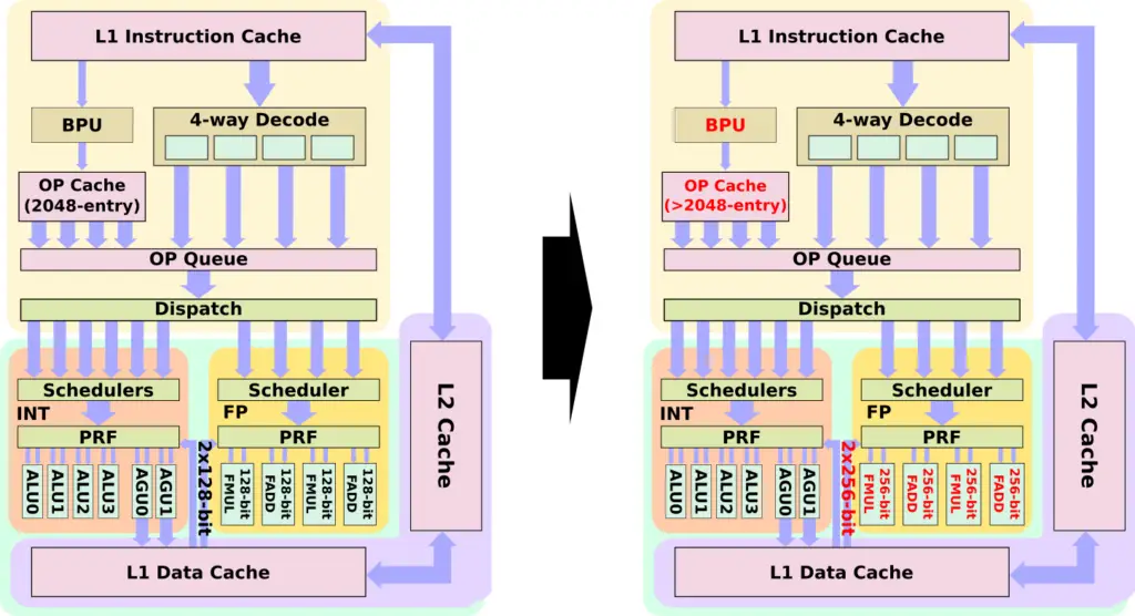
The Epyc 2/Zen 2 architecture with its centralized I/O die obviously was everybody's focus of Zen 2 related design discussions at AMD's Next Horizon event. But there were also some few mentions of changes in the Zen 2 core design which likely have a larger impact on later Ryzen consumer products. I'd like to contrast them with Agner Fog's discussion of bottlenecks in Zen 1's design.
Reading material:


Loops that fit into the μop cache can have a throughput of five instructions or six μops per clock cycle. Code that does not fit into the μop cache can have a throughput of four instructions or six μops or approximately 16 bytes of code per clock cycle, whichever is smaller. The 16 bytes fetch rate is a likely bottleneck for CPU intensive code with large loops.
"Better Instruction Pre-Fetching", "Re-Optimized Instruction Cache", "Larger Op Cache"
-> All three changes should ensure that more code fits the now larger μop cache.
The 256-bit vector instructions are split into two μops each. A piece of code that contains many 256-bit vector instructions may therefore be limited by the number of execution units.
"Doubled Floating Point Width to 256-bit"
-> 256-bit vector instructions in one μop, or doubling of execution units.
The maximum throughput here is four vector-μops per clock cycle, or six μops per clock cycle in total if at least a third of the μops use general purpose registers.
-> Either unchanged four (now 256-bit) or eight (unchanged 128-bit) vector-μops per clock cycle.
-> Probably the former going by the wording in "Doubled Floating Point Width to 256-bit"
Inter-thread communication should be kept within the same 4-core CPU complex if possible.
-> CCX may have been increased to 8 cores and/or inter-CCX latency improved.
Obviously, you cannot execute two instructions simultaneously if the second instruction depends on the output of the first one. It is important to avoid long dependency chains if you want to even get close to the maximum throughput of five instructions per clock cycle.
"Improved Branch Predictor"
-> Better branch predictions should help the core break more dependency chains.
The caches are fairly big. This is a significant advantage because cache and memory access is the most likely bottleneck in most cases. The cache bandwidth is 32 bytes per clock which is less than competing Intel processors have.
"Re-Optimized Instruction Cache", "Larger Op Cache", "Doubled Load / Store Bandwidth", "Increased Dispatch / Retire Bandwidth"
-> For the bigger 256-bit vector instructions these improvements may be a necessity for avoiding new bottlenecks.
"Maintained High Throughput for All Modes"
-> Implies integer and <256-bit vector instructions may also profit from these improvements, possibly significantly so.
Other takes at reading tea leaves, or some rumors going further?
Reading material:
- "The microarchitecture of Intel, AMD and VIA CPUs: An optimization guide for assembly programmers and compiler makers" from Agner Fog's Software optimization resources
- Executive Presentation by Mark Papermaster from AMD Investor Overview
Agner Fog's Microarchitecture page 221 said:20.21 Bottlenecks in AMD Ryzen
The throughput of each core in the Ryzen is higher than on any previous AMD or Intel x86 processor, except for 256-bit vector instructions. Loops that fit into the μop cache can have a throughput of five instructions or six μops per clock cycle. Code that does not fit into the μop cache can have a throughput of four instructions or six μops or approximately 16 bytes of code per clock cycle, whichever is smaller. The 16 bytes fetch rate is a likely bottleneck for CPU intensive code with large loops.
Most instructions are supported by two, three, or four execution units so that it is possible to execute multiple instructions of the same kind simultaneously. Instruction latencies are generally low.
The 256-bit vector instructions are split into two μops each. A piece of code that contains many 256-bit vector instructions may therefore be limited by the number of execution units. The maximum throughput here is four vector-μops per clock cycle, or six μops per clock cycle in total if at least a third of the μops use general purpose registers.
The throughput per thread is half of the above when two threads are running in the same core. But the capacity of each core is higher than what a single-threaded application is likely to need. Therefore, the Ryzen gets more advantage out of simultaneous multithreading than similar Intel processors do. Inter-thread communication should be kept within the same 4-core CPU complex if possible.
The very high throughput of the Ryzen core places an extra burden on the programmer and the compiler if you want optimal performance. Obviously, you cannot execute two instructions simultaneously if the second instruction depends on the output of the first one. It is important to avoid long dependency chains if you want to even get close to the maximum throughput of five instructions per clock cycle.
The caches are fairly big. This is a significant advantage because cache and memory access is the most likely bottleneck in most cases. The cache bandwidth is 32 bytes per clock which is less than competing Intel processors have.
Loops that fit into the μop cache can have a throughput of five instructions or six μops per clock cycle. Code that does not fit into the μop cache can have a throughput of four instructions or six μops or approximately 16 bytes of code per clock cycle, whichever is smaller. The 16 bytes fetch rate is a likely bottleneck for CPU intensive code with large loops.
"Better Instruction Pre-Fetching", "Re-Optimized Instruction Cache", "Larger Op Cache"
-> All three changes should ensure that more code fits the now larger μop cache.
The 256-bit vector instructions are split into two μops each. A piece of code that contains many 256-bit vector instructions may therefore be limited by the number of execution units.
"Doubled Floating Point Width to 256-bit"
-> 256-bit vector instructions in one μop, or doubling of execution units.
The maximum throughput here is four vector-μops per clock cycle, or six μops per clock cycle in total if at least a third of the μops use general purpose registers.
-> Either unchanged four (now 256-bit) or eight (unchanged 128-bit) vector-μops per clock cycle.
-> Probably the former going by the wording in "Doubled Floating Point Width to 256-bit"
Inter-thread communication should be kept within the same 4-core CPU complex if possible.
-> CCX may have been increased to 8 cores and/or inter-CCX latency improved.
Obviously, you cannot execute two instructions simultaneously if the second instruction depends on the output of the first one. It is important to avoid long dependency chains if you want to even get close to the maximum throughput of five instructions per clock cycle.
"Improved Branch Predictor"
-> Better branch predictions should help the core break more dependency chains.
The caches are fairly big. This is a significant advantage because cache and memory access is the most likely bottleneck in most cases. The cache bandwidth is 32 bytes per clock which is less than competing Intel processors have.
"Re-Optimized Instruction Cache", "Larger Op Cache", "Doubled Load / Store Bandwidth", "Increased Dispatch / Retire Bandwidth"
-> For the bigger 256-bit vector instructions these improvements may be a necessity for avoiding new bottlenecks.
"Maintained High Throughput for All Modes"
-> Implies integer and <256-bit vector instructions may also profit from these improvements, possibly significantly so.
Other takes at reading tea leaves, or some rumors going further?