
- Mar 27, 2009
- 12,968
- 221
- 106
Using the processor die maps shown below and the measurement of 169mm2 for quad core + GT3 found in this document, I came up with these Broadwell core size measurements:
Core M = 6.95 mm2
Dual core GT3 = 6.8 mm2 (without dead space included), 8.5 mm2 (with dead space shown in processor die map included)
Quad core GT3 = 6.85 mm2
(Method of taking measurement: I used the outside edge of the outlines as my starting point. Then I measured the total area for both cores on Core M (and the 2C GT3 die) and then divided by two. For the quad core GT3 die, I measure the total area for all four cores and then divided by four.)
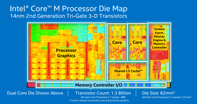
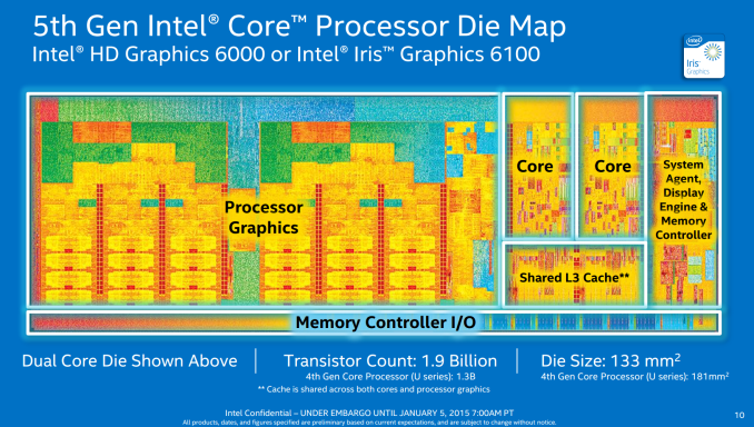
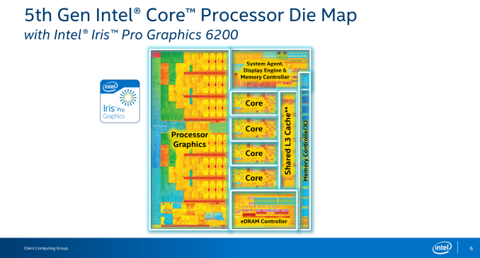
Hopefully we also get a Xeon-D processor die map as I would like to measure those cores as well. However, I feel pretty certain the cores will measure out roughly the same as the ones above.
P.S. The reason I made these measurements was because there was speculation (based on actual statements from Intel) that Core M was using a higher density process than the other Broadwell cores. However, based on the processor core footprint (from these pictures) It doesn't appear to be the case.
Core M = 6.95 mm2
Dual core GT3 = 6.8 mm2 (without dead space included), 8.5 mm2 (with dead space shown in processor die map included)
Quad core GT3 = 6.85 mm2
(Method of taking measurement: I used the outside edge of the outlines as my starting point. Then I measured the total area for both cores on Core M (and the 2C GT3 die) and then divided by two. For the quad core GT3 die, I measure the total area for all four cores and then divided by four.)
Hopefully we also get a Xeon-D processor die map as I would like to measure those cores as well. However, I feel pretty certain the cores will measure out roughly the same as the ones above.
P.S. The reason I made these measurements was because there was speculation (based on actual statements from Intel) that Core M was using a higher density process than the other Broadwell cores. However, based on the processor core footprint (from these pictures) It doesn't appear to be the case.