[BitsAndChips]390X ready for launch - AMD ironing out drivers - Computex launch

Page 20 - Seeking answers? Join the AnandTech community: where nearly half-a-million members share solutions and discuss the latest tech.

Headfoot

Diamond Member
Feb 28, 2008
4,444
641
126
Making a whole new line makes sense when you're:

A) On a new node and want to extract performance from that node, or
B) Have made major architectural advances (eg. G71 -> G80, Kepler -> Maxwell)

If Fiji is just minor enhancements + HBM, it wouldn't make much sense to scale it down for the rest of the market. HBM is almost certainly too expensive for budget SKUs so you'd be looking at significant cost for minimal gain.

HBM is a major change. Come on. The biggest change in memory since the invention of a G(raphics) spec of DDR.
 

HurleyBird

Platinum Member
Apr 22, 2003
2,815
1,552
136
HBM is a major change. Come on. The biggest change in memory since the invention of a G(raphics) spec of DDR.

Don't put words in my mouth. I never said HBM wasn't a major change, just that it's likely too expensive right now to build a top-to-bottom product stack around.
 

HurleyBird

Platinum Member
Apr 22, 2003
2,815
1,552
136
It is, just doesnt make much sense before HBM2. HBM1 should have stayed as a prototype.

That's an awful lot of confidence for such a speculative opinion. I guess you haven't learned from your past history. We'll see when Fiji comes out how much of an impact HBM1 has. Until then, saying that only HBM2 makes sense is premature.
 

ShintaiDK

Lifer
Apr 22, 2012
20,378
146
106
That's an awful lot of confidence for such a speculative opinion. I guess you haven't learned from your past history. We'll see when Fiji comes out how much of an impact HBM1 has. Until then, saying that only HBM2 makes sense is premature.

HBM1s main advantage is power consumption. Its disadvantage is price.

Speed wise HBM1 and GDDR5 is about equal. 4 stacks(4096bit) 1Ghz HBM=512GB/sec. GDDR5 8Ghz 512Bit=512GB/sec.
 

Enigmoid

Platinum Member
Sep 27, 2012
2,907
31
91
HBM1s main advantage is power consumption. Its disadvantage is price.

Speed wise HBM1 and GDDR5 is about equal. 4 stacks(4096bit) 1Ghz HBM=512GB/sec. GDDR5 8Ghz 512Bit=512GB/sec.

You can scale HBM way beyond GDDR5.

Not to mention that a 512 bit 8 ghz GDDR5 bus will use a ton of power and take up a lot of room making it highly undesirable.

HBM is less useful on the lower end but an absolute on the high end if you want to increase performance.
 

HurleyBird

Platinum Member
Apr 22, 2003
2,815
1,552
136
HBM1s main advantage is power consumption. Its disadvantage is price.

Speed wise HBM1 and GDDR5 is about equal. 4 stacks(4096bit) 1Ghz HBM=512GB/sec. GDDR5 8Ghz 512Bit=512GB/sec.

1) It's likely that the HBM in Fiji is clocked at 1.25GHz, making 640GB/s bandwidth.
2) The power consumption advantage is likely very significant.
3) A 512-bit controller that is refined enough to handle 512GB/s+ bandwidth is going to take up an enormous amount of die space. HBM will probably take up significantly less.
4) It's not just about bandwidth. HBM is significantly lower latency than GDDR5, how that will affect Fiji's performance is a bit of an unknown factor.
 

ShintaiDK

Lifer
Apr 22, 2012
20,378
146
106
1) It's likely that the HBM in Fiji is clocked at 1.25GHz, making 640GB/s bandwidth.
2) The power consumption advantage is likely very significant.
3) A 512-bit controller that is refined enough to handle 512GB/s+ bandwidth is going to take up an enormous amount of die space. HBM will probably take up significantly less.
4) It's not just about bandwidth. HBM is significantly lower latency than GDDR5, how that will affect Fiji's performance is a bit of an unknown factor.

Hynix isnt selling any 1.25Ghz HBM1 chips. And they go up in steps of 200Mhz, not 250Mhz. The current only stacked memory at 1.25Ghz is Microns HMC.

I dont think gaming depends much on latency.
 

RussianSensation

Elite Member
Sep 5, 2003
19,458
765
126
Speed wise HBM1 and GDDR5 is about equal. 4 stacks(4096bit) 1Ghz HBM=512GB/sec. GDDR5 8Ghz 512Bit=512GB/sec.

You make it sound like:

1) The extra power usage of GDDR5 8Ghz over 512-bit controller is immaterial. Yes, I am sure AMD should just waste 50W of TDP on the exact same memory bandwidth. Who cares about 50W of extra power usage, not like it can be used for making the GPU faster..... :whiste:

AMD-HBM-Die-Stacked-Memory.jpeg


How do you not realize that with 50W less power usage from memory alone, AMD can increase GPU clocks/make a much larger chip?

2) You make it seem like designing a 512-bit controller that can run 8Gbps GDDR5 is a peace of cake. Is that why NV is still stuck on 384-bit and 7Ghz with the Titan X? How do you not understand that after Fermi GDDR5 clock speed issues NV faced that took 2 years to resolve with Kepler's GDDR5 memory controller, that it's not as simple as just combining the fastest GDDR5 with any memory controller? :whiste:

3) You assign no value at all to AMD having a full generation of experience with HBM which will make it easier for their engineers to transition to HBM 2.0 next gen.

The amazing part is you never admit how flawed your assumptions/arguments are even after you are proven wrong, which is more or less assured since R9 390X will have HBM and memory bandwidth exceeding any GDDR5 card to date.

I dont think gaming depends much on latency.

I don't even...

You can scale HBM way beyond GDDR5.
Not to mention that a 512 bit 8 ghz GDDR5 bus will use a ton of power and take up a lot of room making it highly undesirable.
HBM is less useful on the lower end but an absolute on the high end if you want to increase performance.

Don't worry, once a certain team adopts HBM 2, HBM will be the next best thing since sliced bread.

"1GB HBM package size is smaller than 1 tablet of aspirin. DDR4 is 37X bigger" - Slide 14

I guess he knows better though vs. engineers who get paid 6 figures to design next gen memory tech.
http://www.memcon.com/pdfs/proceedings2014/NET104.pdf

Even at “standard” 1Gb/s per-pin data-rate the memory sub-system will feature 512GB/s bandwidth. Add Tonga's 40% higher memory bandwidth efficiency, and R9 390X based on GCN 1.2 architecture with 512GB/sec HBM1 would have an "effective/equivalent R9 290X memory bandwidth" of 717 GB/sec.

ColorCompress.png


I wonder what all those AMD engineers get paid $ for when they could have just paired 8Gbps GDDR5 with Hawaii's 512-bit bus and called it a day.....instead they wasted 1.5 years working with SK Hynix on next gen HBM memory - all of them should be fired................/sarcasm.
 
Last edited:

.vodka

Golden Member
Dec 5, 2014
1,203
1,538
136
Stop feeding the troll, RS. He won't understand.

Computex gets closer every day! As long as AMD in its actual shape can (and will) produce a card faster than 290x that consumes less power (or similar), and gets close enough (or surpasses) the X... it'll be fine. There is evidence to see it's possible for them to pull off such a thing. Pricing will make or break the new series, of course.

*If* it beats the X... Well, what else can be said about GCN. It'll be hard for them to come up with a better architecture, that could last as long..

Warning issued for member callout.
-- stahlhart
 
Last edited by a moderator:
Feb 19, 2009
10,457
10
76
HBM1s main advantage is power consumption. Its disadvantage is price.

Speed wise HBM1 and GDDR5 is about equal. 4 stacks(4096bit) 1Ghz HBM=512GB/sec. GDDR5 8Ghz 512Bit=512GB/sec.

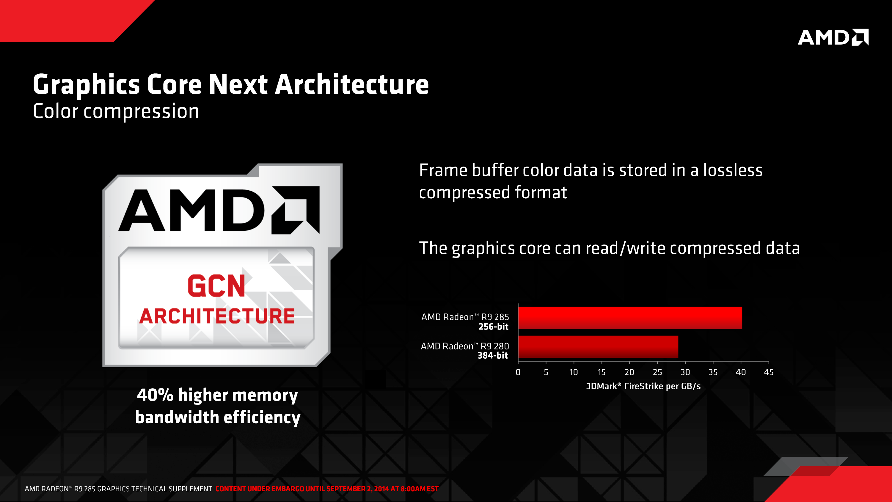
If we forget about the fact that driving GDDR5 at 8ghz over a 512 bit bus is very power demanding as well as die space consuming, yeah, its equal.

It's been publicly said that GDDR5 memory subsystem is 1/5th to 1/3rd (depending on the bus size) of the die area as well as overall TDP.

Note that any power savings as well as die space savings from HBM can be devoted to performance.

Latency matters for computing & rendering, due to multiple pass required (shadow, bump maps, lighting, post effects and much more) to render a complex scene, inbetween, that data is shuffled around. Lower latency => higher uptime on shaders and less idle cycles resulting in increased efficiency or IPC per shader, thus, overall performance.

Also, R290/X isn't competing versus 970/980. It's the reason for the major marketshare loss for AMD. The average buyer sees that the R290X system uses 100W more, they avoid it and willing to pay extra for less performance/crippled vram 970. Thus, to "rebrand" it to further compete with 970/980 for the next cycle is suicidal.

And Tonga XT is a stop-gap, a test measure, which AMD is lucky to pawn off to Apple. It does not significantly improve efficiency or performance over Tahiti to make it competitive. AMD needs a "Maxwell leap" of their own in order to compete. Tonga is not going to compete well in the segment where the 960/XT occupies as long as it uses much more power.

So, re-branding products that aren't selling and failing to be competitive and asking them to compete for the next cycle? No. Only utter newbies would even think of such a move. I have doubts that AMD is that stupid.
 

RussianSensation

Elite Member
Sep 5, 2003
19,458
765
126
Stop feeding the troll, RS. He won't understand.

I don't understand how someone can be so against next generation technologies such as HBM. It's similar to how some people are hating on DDR4. Sure, in the early stages DDR4 won't show big advantages over DDR3 but over time, just like DDR2 superseded DDR1 and DDR3 superseded DDR2, DDR4 and HBM will become the future until they are replaced by more advanced tech.

Computex gets closer every day! As long as AMD in its actual shape can (and will) produce a card faster than 290x that consumes less power (or similar), and gets close enough (or surpasses) the X... it'll be fine. There is evidence to see it's possible for them to pull off such a thing. Pricing will make or break the new series, of course.

A popular mid-range card today uses 168W on average and 192W at peak.

Let's use 80% power usage for the 2nd one due to 80% dual-GPU scaling --> we get 168W x 1.8 = 302W average and 192W x 1.8 = 347W peak.

Now hypothetically, imagine if a 300-350W R9 390X gives us 87-90% of $650 dual card performance at $700? Winning!

However, against R9 290 CF for $480, R9 390X will find itself in a much tougher position for price/performance.
 
Last edited:

Head1985

Golden Member
Jul 8, 2014
1,867
699
136
AMD needs a "Maxwell leap" of their own in order to compete. Tonga is not going to compete well in the segment where the 960/XT occupies as long as it uses much more power.

So, re-branding products that aren't selling and failing to be competitive and asking them to compete for the next cycle? No. Only utter newbies would even think of such a move. I have doubts that AMD is that stupid.
Of course AMD is not stupid.They simple dont have money to do that.
AMD RnD 238M - http://ycharts.com/companies/AMD/r_and_d_expense
NV RnD 348M - http://ycharts.com/companies/NVDA/r_and_d_expense

AMD develop CPU,GPU and APU at the same time.NV only GPU.I think its not that crazy saing AMD GPU division have 15-20% of NV budget.
They simple cant compete with them and thats why we have here 7months maxwell without competetion.I am pretty sure AMD want compete with maxwell but they just dont have new cards ready.
 
Feb 19, 2009
10,457
10
76
Of course AMD is not stupid.They simple dont have money to do that.
AMD RnD 238M - http://ycharts.com/companies/AMD/r_and_d_expense
NV RnD 348M - http://ycharts.com/companies/NVDA/r_and_d_expense

AMD develop CPU,GPU and APU at the same time.NV only GPU.I think its not that crazy saing AMD GPU division have 15-20% of NV budget.
They simple cant compete with them and thats why we have here 7months maxwell without competetion.I am pretty sure AMD want compete with maxwell but they just dont have new cards ready.

So when Fermi was 9 months late, was it because NV lacked the $ for R&D?

If you want to apply logical thinking, you can't ignore recent history.

ps. Pretty sure NV's expansion into cars, mobiles, servers means more expenditures on other things besides their core product: GPUs.
 

RussianSensation

Elite Member
Sep 5, 2003
19,458
765
126
So when Fermi was 9 months late, was it because NV lacked the $ for R&D?

;)

HD5850 = $259 Sept 30, 2009
GTX460 = $200 Jul 11, 2010 (+285 days)

vs.

GTX980 = $550 Sept 18, 2014
R9 390 series = ? (June 30, 2015 > +285 days)

Key point: 460 lost to a 5850 by 15% at 1080P and by 23% at 1600P. $60 saved to wait 285 days and get 15-23% lower performance. 460 = hailed revolutionary. D:

The number of threads/posts about the company launching late, not competing/going bankrupt any minute now? Can hardly remember any. :rolleyes:
 
Last edited:
Feb 19, 2009
10,457
10
76
So back when NV's R&D budget were tiny, they could afford multiple designs and in fact had many SKUs...

But somehow, AMD can't? That's your conclusion that it has to be a rebrand due to a 1.2B a year budget that cannot produce multiple variants of a micro architecture?

Grasping at straws much?

ps. Fermi paper launch does not hide the fact it was a failure, which isn't due to NV's R&D or lack of, but TSMC's failure on a new node. Perhaps AMD is late because they are transitioning to GF and that hasn't gone according to schedule?

Infraction issued for thread crapping.
-- stahlhart
 
Last edited by a moderator:

stahlhart

Super Moderator Graphics Cards
Dec 21, 2010
4,273
77
91
For the third -- and last -- time, THIS THREAD IS FOR DISCUSSING NEXT GENERATION AMD HARDWARE, NOT NVIDIA. STOP DERAILING IT.
-- stahlhart
 
Feb 19, 2009
10,457
10
76
We ARE discussing next gen GPUs from AMD. It's directly related to why it's late and that's the current topic.

It's as far from thread crapping as you can imagine because without concrete info relating to products about to launch to speculate on, the only thing left to discuss is why it's late & whether HBM will provide tangible benefits, whether its a rebrand (& late!)... which is what we're doing.

Unless you have a better topic regarding AMD's next-gen, feel free to move the discussing that way.

I think why they are so late is a big deal.


If you have an issue with the moderation, make an MD thread.

To counteract a mods instruction in the thread is considered mod callout.


esquared
Anandtech Forum Director
 
Last edited by a moderator:

RussianSensation

Elite Member
Sep 5, 2003
19,458
765
126
It's as far from thread crapping as you can imagine because without concrete info relating to products about to launch to speculate on, the only thing left to discuss is why it's late & whether HBM will provide tangible benefits, whether its a rebrand (& late!)... which is what we're doing.

Let's consider this, isn't R9 380/380X supposed to be called Grenada?

When AMD re-branded R9 280/280X, they didn't come up with new names for them. They were still called Tahiti. Similarly, HD7870 became R9 270/270X but still called Pitcairn.
http://www.anandtech.com/show/7400/the-radeon-r9-280x-review-feat-asus-xfx

If R9 380/380X are re-brands, why is AMD changing the codename from Hawaii to Grenada? It would only make sense if it's new silicon with some changes such as the move to GCN 1.2 or even 1.3, newer re-spin of a 28nm node (with new perf/watt characteristics), possibly different GPU clocks.

I mentioned a while back that you can just make a GCN 1.2 or 1.3 card with the same number of SP/TMU/ROP configuration of an R9 290/290X. If someone just released paper specs, you would think that R9 380/380X would be 100% identical to Hawaii. However, without knowing if R9 380/380X are GCN 1.2 or 1.3, what their 28nm transistor properties are (GloFo vs. TSMC vs. more mature node re-spin), and without knowing their die sizes/transistor count (die size could grow to incorporate GCN 1.2/1.3 changes due to improved colour fill-rate, pixel fill-rate and geometry performance), on paper the 380/380X and 290/290X could appear identical but perform differently.

It would make more sense for AMD to rename a Hawaii chip Grenada if there were significant changes to the chip itself, even if the specs are identical to 290/290X otherwise.

Imagine if we only knew SPs, TMUs, ROPs and GPU clock of HD5770 vs. 4770. It would be easy to falsely conclude that 5770 is nothing but a 4770 re-brand with higher GPU clocks.

What if AMD incorporated a new aggressive PowerTune/Boost technology? We would have no clue about it based on paper specs alone.
 

RussianSensation

Elite Member
Sep 5, 2003
19,458
765
126
You mean 4870?

Ya, my bad. Thanks for correcting me. That link has a 4870. :thumbsup:

I'll expand on my point though. If we look at R9 285 vs. R9 290 on paper, there is no way to explain how 285 creams 290 in geometry and pixel fill-rate performance.

1. R9 285 and 290 = both can do 4 rasterized triangles/clock, which means at 285's lower clock speed of 918mhz it's losing to a 947-1Ghz 290/290X

2. R9 290X smokes the 285 in integer and FP16 texels filtered per clock (176/88 vs. 128/64 for the 285)

3. R9 290X has 64 ROPs vs. 32 ROPs for the 285. This is the most shocking part of all - 100% more pixel fill-rate on paper but 290 loses.

4. R9 290X has 320GB/sec memory bandwidth vs. only 176GB/sec for 285. We know memory bandwidth is very important in feeding the ROPs, but again 290 loses in real world pixel fill-rate performance! WOW.

5. Each shader engine in the 285 has only 8 Compute Units for a total of 32. In contrast, R9 290X has 11 Compute Units in each shader engine for a total of 44.

So what's the deal then? On paper, 285 should be losing everywhere.

tm-x32.gif


67234.png


^ Where is this coming from? Not from on paper specs. That's why even if we knew that R9 380/380X had identical SP/TMU/ROP and memory bus width to 290/290X, without knowing their die sizes and transistor count, we can't say if they are re-brands.
 
Last edited:
Feb 19, 2009
10,457
10
76
The only people who believe AMD will rebrand most of the mid-range/high-end lineup are those who like to think AMD is too stupid to see reality, that Tahiti, Pitcairn, Tonga and Hawaii are not competitive versus Maxwell... so they will push them out again to compete for the next cycle..

Yeah, really? Lisa cannot be that clueless.
 

JDG1980

Golden Member
Jul 18, 2013
1,663
570
136
I think this forum needs to have a clear definition of what the term re-branding means because this is partly what's creating the confusion.

For example, do we mean re-branding as in "re-badging" such as when HD5750/5770 became HD6750/6770 with absolutely 0 changes? Or are we using the term re-branding to mean taking an existing architecture/SKU and improving upon the predecessor as in HD4870 to HD4890?

I would not use the term re-branding for HD4890 even though underneath it's an identical architecture to the HD4870. It sounds to me like some people in this thread are using the term so loosely that they would call a Hawaii-based R9 380X with 10% faster clocks and 10% lower power usage a "re-brand."

My position is simple: if the silicon coming off the wafers is unchanged, then it's a rebrand. When AMD switched from the HD 7870 to the R9 270X with the same silicon but higher RAM clocks (and higher power usage), that was a rebrand. When AMD released the R7 260, that was also a rebrand; even though that specific configuration of Bonaire (two CUs disabled) had never been released before, it was still the same silicon coming off the wafers. Likewise, if AMD releases a fully enabled Tonga as part of the 300 series, that card will be a rebrand even though the full Tonga hasn't yet seen release as a stand-alone desktop card. The silicon coming off the wafers is the same, so it's a rebrand.

If AMD were to respin Tonga for GloFo instead of TSMC and got lower power consumption at the same clocks, then that wouldn't be a rebrand, because it would be different silicon. If they decide to die-shrink Tonga next year, that won't be a rebrand either (though it would be disappointing to see no other improvements in that time). If AMD created a new GPU that happened to have the same stats as Pitcairn (1280 SPs, 80 TMUs, 32 ROPs, and a 256-bit bus width), but incorporated GCN 1.2+ architecture, then that definitely wouldn't be a rebrand - it would be a new chip that is designed as a replacement to an existing one.
 

Enigmoid

Platinum Member
Sep 27, 2012
2,907
31
91
Let's consider this, isn't R9 380/380X supposed to be called Grenada?

When AMD re-branded R9 280/280X, they didn't come up with new names for them. They were still called Tahiti. Similarly, HD7870 became R9 270/270X but still called Pitcairn.
http://www.anandtech.com/show/7400/the-radeon-r9-280x-review-feat-asus-xfx

If R9 380/380X are re-brands, why is AMD changing the codename from Hawaii to Grenada? It would only make sense if it's new silicon with some changes such as the move to GCN 1.2 or even 1.3, newer re-spin of a 28nm node (with new perf/watt characteristics), possibly different GPU clocks.

To that end this means we’re still going to be looking at the same GCN feature set schism. R9 280X and R9270X are of course based on the original GCN architecture, while the Bonaire powered R7 260X is based on AMD’s revised GCN architecture. Since AMD has still not officially assigned names to these architectures, and because “Sea Islands” has been badly mangled by now, we’re going to continue referring to these architectures as GCN 1.0 and GCN 1.1 respectively. At least until such a time where they get a proper name out of AMD.

With that said, while AMD is doing their best to drop codenames, they are technically still alive and kicking. Our R9 270X reference card is labeled Curacao, for example, despite the fact that it’s based on the venerable Pitcairn GPU. So AMD still has codenames internally, apparently including new names for existing GPUs.

From the same anandtech link.