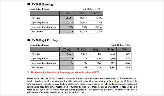
Seems this might be a valid leak from inside partner SK Hynix..
Twitter
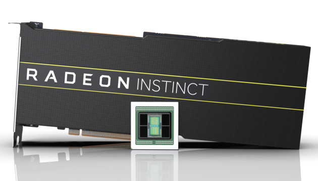
Big Navi - Radeon 5950XT: Twice the compute units as Navi 10.
Shading units: 5120
TMUs: 320
Compute units: 80
ROPs: 96
L2 cache: 12MB
Memory: 24GB (4 x HBM2e, 3 die)
Memory bus: 4096 bits
Band Width: 2048 GB/s

All these Big Navi numbers are perfectly consistent. The 96 ROPs are tiny pieces of logic at the edge of the memory tiles of the 12MB L2 cache which explanes the factor 3 in these numbers. An old example here https://bjorn3d.com/2010/01/nvidia-gf100-fermi-gpu/
SK Hynix will make 6GB HBM2e stacks with 3 dies per stack for consumer applications on request. SK Hynix recently announced HBM2e at 512GB/s at ISSCC-2020. Samsung went a step further with 640GB/s HBM2e (5 Gb/s/pin)

Big Navi - Radeon 5950XT: Twice the compute units as Navi 10.
Shading units: 5120
TMUs: 320
Compute units: 80
ROPs: 96
L2 cache: 12MB
Memory: 24GB (4 x HBM2e, 3 die)
Memory bus: 4096 bits
Band Width: 2048 GB/s
All these Big Navi numbers are perfectly consistent. The 96 ROPs are tiny pieces of logic at the edge of the memory tiles of the 12MB L2 cache which explanes the factor 3 in these numbers. An old example here https://bjorn3d.com/2010/01/nvidia-gf100-fermi-gpu/
SK Hynix will make 6GB HBM2e stacks with 3 dies per stack for consumer applications on request. SK Hynix recently announced HBM2e at 512GB/s at ISSCC-2020. Samsung went a step further with 640GB/s HBM2e (5 Gb/s/pin)