Discussion Beyond zen 6

Page 5 - Seeking answers? Join the AnandTech community: where nearly half-a-million members share solutions and discuss the latest tech.

Doug S

Diamond Member
Feb 8, 2020
3,820
6,754
136
I mean 3d cache stacking. (the way the L3 cache works now) An L2 would never work with that level of latency. Seriously. It increased the already slow L3 to a few ticks slower and I'm sure there is some secrete logic sause where the faster L3 makes up for the slower stacked part.

Think of it in terms of wire length. If you have a cache block that's x in width sitting to the side of a core the average wire length it needs to traverse from the edge of the core is x/2. If you have the cache sitting on top so that the middle of the block sits on the edge of the core (wherever the "path" is deemed to begin) then the average wire length is x/4 + the vertical distance. Given that the vertical distance is pretty small compared to the half width of a cache block your average wire length for stacked cache will be shorter.

Now I know I'm oversimplying some here, and handwaving over details like the spacing of TSVs that connect the cache die to the main die, but I think those are just details while the overall example remains applicable.
 

Joe NYC

Diamond Member
Jun 26, 2021
4,200
5,780
136
you do understand that GPU caches are very different things built for very different reasons?
They have latency in tens or hundreds of cycles.

Shouldn't that then make it easier to use stacked L2? Especially if AMD has (or is going to have) a method that is also very power efficient, not incurring penalty for going across dies?

It's cheap given what those things will retail for. That's it.

N4 will be cheaper and more available in 2026, 2027. There must be a good reason why AMD is going with a more expensive N3.

AMD ain't paying any less for HBM4, they're just not willing to deal with the thermal nightmare of 11Gbps HBM4 at the current DRAM nodes.

I am pretty sure AMD will be paying less for lower bins, those that failed NVidia cut off but are good enough for AMD.
 

adroc_thurston

Diamond Member
Jul 2, 2023
8,486
11,203
106
Shouldn't that then make it easier to use stacked L2?
Guess what Ponte Vecchio had bruddah
There must be a good reason why AMD is going with a more expensive N3.
It's a no holds barren product.
How is this a question?
I am pretty sure AMD will be paying less for lower bins, those that failed NVidia cut off but are good enough for AMD.
No, they have very different qualification metrics.
 

Joe NYC

Diamond Member
Jun 26, 2021
4,200
5,780
136
Guess what Ponte Vecchio had bruddah

Stacked cache without SoIC is not really in the same category.

It's a no holds barren product.
How is this a question?

AMD should be gaining more on NVidia from having a whole base die that it currently is. Maybe the base die in Mi455 will finally bring home the bacon.

Similarly to what V-Cache does for the CPUs
 

Joe NYC

Diamond Member
Jun 26, 2021
4,200
5,780
136
Kind of? It's a lot more relevant for trad HPC.

Going from L2 scarcity to L2 abundance, design decisions can change to take advantage of it. And it could make it to client too by RDNA6 or RDNA7. We could see a stacked GPU dies for both chiplets and dGPUs.
 
  • Like
Reactions: Hulk

itsmydamnation

Diamond Member
Feb 6, 2011
3,130
3,985
136
Going from L2 scarcity to L2 abundance, design decisions can change to take advantage of it. And it could make it to client too by RDNA6 or RDNA7. We could see a stacked GPU dies for both chiplets and dGPUs.
if we go by AMD comments they are not blowing up the memory hiearchy every design anymore , its to hard to get consistant performance, so unless they implement stacked L2 cache in every market/ every product we will see the same reg file/LDS/L0/L1/L2/L3/whatever ratio/designs for shader cores and gpus.


edit: this is from the same interview that UDNA came from and was one of the actual intents when explaning what was meant by UDNA , not the unified shader core people ran with.
 
  • Like
Reactions: Tlh97 and marees

Joe NYC

Diamond Member
Jun 26, 2021
4,200
5,780
136
if we go by AMD comments they are not blowing up the memory hiearchy every design anymore , its to hard to get consistant performance, so unless they implement stacked L2 cache in every market/ every product we will see the same reg file/LDS/L0/L1/L2/L3/whatever ratio/designs for shader cores and gpus.

What are the odds that stacked die will become as much a norm (at least for AMD) as was the chiplet design started with Zen?

If you take the current trends / leaks for Zen 6, every client chip except one (MDS1) is a chiplet based, that will need advance packaging.

The advanced packaging adds some costs, as does SoIC 3D stacking. Just adding SoIC alone is a cost adder. But replacing other advanced packaging with SoIC = offsetting costs.

So in theory, what seemed like a far fetched scenario, of future client chips looking like Mi300-Mi455 design may be closer to reality than before.

If stacked L2 + L3 can secure unparalleled CPU performance, it's an attractive proposition to proliferate it across all segments. You can just add bunch more stuff from a notebook chips to the base die, including IO, memory controllers and then have just core complexes (CPU and GPU) sitting on top of this base die and be much smaller consumption of the most advanced process silicon offset by die on the cheaper node for base die. It's just that it is a little more complex in notebook chips than in server / desktop CCDs.

In general, there are a number of barriers holding you back from achieving higher performance. AMD leadership figured out that the best way is to apply maximum pressure to the easiest to move barrier. Which is how AMD gained server CPU leadership with EPYC, applying the max pressure on increasing the chiplets.

Stacked L3 was very similar scenario. To increase L3 size through stacking, which was a weaker barrier than growing the chip size to increase L3.

If the CPUs CCDs (desktop and server) are already in process of transitioning to 2 stacked die design (single die CCD may disappear) than it is a non-brainer to also add L2 to the stacked die.

if some 33% Zen 5 die (minus SerDes) is SRAM, and a 16 core Zen 7 die would normally be 100 mm2, then moving both L2 and L3 off the base die would shrink the chip to 66mm2.

Then, the remaining 33mm2 moved to stacked die would increase to 66mm2, with enough room to place 2x L2 and 2x L3. In other words, 2MB L2 per core and 8 MB L3 per core. That would maintain the cache hierarchy.
 

Joe NYC

Diamond Member
Jun 26, 2021
4,200
5,780
136
if we go by AMD comments they are not blowing up the memory hiearchy every design anymore , its to hard to get consistant performance, so unless they implement stacked L2 cache in every market/ every product we will see the same reg file/LDS/L0/L1/L2/L3/whatever ratio/designs for shader cores and gpus.

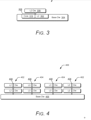
BTW, I just looked at the charts and figures from the patent application, discovered by @Kepler_L2

In particular, Figure 3, that shows a compute die with Core and L2, and there is additional L2 that is on stacked die. That could in fact be the biggest game changer, which AMD could implement much sooner than many expect. In theory, not even having to go "Beyond Zen 6" as the thread title says. AMD could surprise us by including it in Zen 6 V-Cache.

And, unlike your concern, it would not blow up the cache hierarchy. AMD would not have to wait until there is a CPU designed from ground up to be a 2 die CPU. Instead, AMD could sell a perfectly fine Zen 6, with 2 MB L2 and the V-Cache die can add another 2 MB.

Figure 4 shows stacked die having both L2 and L3.


1768892144866.png
 
  • Like
Reactions: lopri and Tlh97

Joe NYC

Diamond Member
Jun 26, 2021
4,200
5,780
136
Zen6 has the exact same 1M L2 slab as Zen4.

I see, I may be confusing it with the Zen 7 leaks.

Which brings up another question. If Zen 7 V-Cache is to go from 8MB to 10MB V-Cache, I wonder if it is 2MB L2 + 8 MB L3 on V-Cache die.
 
Last edited:

Joe NYC

Diamond Member
Jun 26, 2021
4,200
5,780
136

Well, it was in the MLID video.

nerd dreams like these exist to be pulverized by the harsh reality of it.
You're getting 2M L2 slab for Zen7 and that's it. enjoy!

If V-Cache die has 10 MB per core, and Zen 7 goes to 2 MB L2. Doesn't it seem like there is possible that L3 in V-Cache stays at 8M, as it has been since Zen 3 (even though there was an opportunity to increase in in Zen 5) and the other 2 MB complement on die L2?

In MLID video, he states that cache alone is going to add 8% of performance on Zen 7 (as one of the highlights).
 

LightningZ71

Platinum Member
Mar 10, 2017
2,689
3,383
136
The poor don't make them any money. Why would they invest in them? I also contend that the 8CU iGPU in KRK is enough for casual 1080p gaming with FSR 3.x. Incremental upgrades to it aren't going to move the needle in a meaningful way.

AMD had a chance with STXp with a 16MB MALL cache that would have given better than 6500XT performance in most cases, but bailed on it for a useless NPU.
 
  • Like
Reactions: ToTTenTranz

branch_suggestion

Senior member
Aug 4, 2023
889
1,939
106
This isn't really uncore-related.
It's just whether or not gfx ppl impact the GEMM brrr race before or after 2029.
So it comes down to the timing of the NPU being depreciated.
Well then it is still gonna be in flux for a while before a final decision is made, zero reason why RDNA5 couldn't be put in it otherwise.
 

adroc_thurston

Diamond Member
Jul 2, 2023
8,486
11,203
106
So it comes down to the timing of the NPU being depreciated.
Well then it is still gonna be in flux for a while before a final decision is made, zero reason why RDNA5 couldn't be put in it otherwise.
Not deprecated, gutted.
It's still very useful for always on ML slop.
GPUs just do the perf stuff better and have wider support and stuff.

RDNA5 should generally be viable for poverty stuff anyway since they gut every last SRAM bitcell there is.
 

Fjodor2001

Diamond Member
Feb 6, 2010
4,598
739
126
Not deprecated, gutted.
It's still very useful for always on ML slop.
GPUs just do the perf stuff better and have wider support and stuff.

RDNA5 should generally be viable for poverty stuff anyway since they gut every last SRAM bitcell there is.
Then why is MS requiring NPU for Copilot+? That is not (only) always on stuff.

Also, in the end it’s TOPS that matters, not whether it comes from NPU or (i)GPU. So if NPU can deliver the TOPS needed, what’s the problem?
 

LightningZ71

Platinum Member
Mar 10, 2017
2,689
3,383
136
MS is pushing a subscription sales model. They wanted an always on AI component in Windows that you were willing to pay for. If it drained your battery rapidly or worked like dog excrement, no one would buy it. The NPU helps with both.
 

marees

Platinum Member
Apr 28, 2024
2,238
2,874
96
MS is pushing a subscription sales model. They wanted an always on AI component in Windows that you were willing to pay for. If it drained your battery rapidly or worked like dog excrement, no one would buy it. The NPU helps with both.
you get battery saving only for low throughput (& always on) kind of tasks. for high throughput GPUs should be better.

i am not convinced that NPUs are needed