Architectural Direction of GPUs

Page 3 - Seeking answers? Join the AnandTech community: where nearly half-a-million members share solutions and discuss the latest tech.

HurleyBird

Platinum Member
Apr 22, 2003
2,684
1,267
136
Which is still demonstratably false with all the reviews showing the GTX 480 as beating the 5870 in games, while having the theoretical fillrate disadvantage.

-snip- none of this stuff please. -KP

EDIT: KP: Ok fair enough, but if you want to snip this you may as well snip the rest of the posts in this particular discussion!

You can get your points across in better ways. If you can't, you will not participate in this thread. There is no room and more importantly, no reason for anything else in this requested heavily moderated thread. If you are determined to make a comeback comment, it would be your last in this thread. -KP

EDIT: Sure, I'll let it go then. Might shoot you a PM later.

But yeah, card with the highest fillrate being the fastest is merely coincidental here, as a theoretical Fermi dual chip card (assuming it's even possible to dissipate that much power in such a small area) would be king with lower fillrate.
 
Last edited:

konakona

Diamond Member
May 6, 2004
6,285
1
0
Surprisingly though, fermi seems to OC rather well from what I have seen so far and the gains are typically bigger than OC'ing cypress, sometimes by quite a lot. Loud and expensive yes, but performance is better than expected.
 

ArchAngel777

Diamond Member
Dec 24, 2000
5,223
61
91
I disagree with this statement. I believe there are very few people with a single 1920 x 1200 who would be or should be in the market for a $500 video card since it is overkill for their needs. So in all honesty 2560 x 1600 or dual screen should be the standard by which these cards are judged.

1920 x 1200 might be a good benchmark for a step down in the 300-350 range where the 5850 and 470 compete however.

I will challenege your statement. Lets ask the question another way. Out of all the people who own a GTX 480, do more than 50% have a 2560x1600 display? I would say no way... However, since I don't have access to that data (not sure anyone does) I can't refute your claim, just that I highly doubt that even 10% of people who have a GTX 480 have a display higher than 1920x1200. Speak up if you have evidence to the contrary. But if I am right, it means that 1920x1200 is the perfect and ideal resolution to shoot for on a high-end card.

In any case, exceeding the fill rate requirements for 2560x1600 seems like overkill and would only affect a very small part of an already tiny market. Of course as displays get larger, or higher DPI, then it makes sense at that time. Not to mention that if you were lacking the fill rate to play at 2560x1600, you can always go dual GPU or what not.

I am not saying that more fill rate is bad, but at some point it is excessive and wouldn't do good for 99.99% of users. nVidia has to make money, ATI has to make money... IMO they aim for the 1680x1050 and 19200x1200 market, and give a solution for the 2560x1600 market via SLI or XFIRE.
 

ArchAngel777

Diamond Member
Dec 24, 2000
5,223
61
91
Ummm... forgetting 5970 much?

This kind of comment does not belong here in this discussion. But to address your point. I did not forget about it, but sandwich cards are a inique animal and generally never taken into consideration in my discussions. But, regardless, for a single GPU, the fastest card is not always the one with the highest fillrate, as is the case with the GTX 480.
 

ArchAngel777

Diamond Member
Dec 24, 2000
5,223
61
91
Could the reason for the relatively large fill rate on 5xxx be Eyefinity support? Even at a lowly 1680x1050, three monitors would require ~30% more pixels than a single one at 2560x1600.

Very good point! Yes, I would agree with this. In these situations, the fillrate of the 5870 makes sense and is perhaps the reason for it to begin with.
 

HurleyBird

Platinum Member
Apr 22, 2003
2,684
1,267
136
Surprisingly though, fermi seems to OC rather well from what I have seen so far and the gains are typically bigger than OC'ing cypress, sometimes by quite a lot. Loud and expensive yes, but performance is better than expected.

Yeah, it is interesting, but the question I have is how much of this is due to Fermi scaling well with added frequency, and how much of this is due to Cypress scaling badly. Just as interesting to me than how well Fermi scales Vs. Cypress would be how well Fermi scales Vs. GT200.

In terms of Cypress scaling, something very fishy is happening. ABT just did an article comparing a 5870 OC'ed 975/1300 to an OC'ed GTX 480 and half of the time it barely made a dent in the numbers -- like, less than a percent -- while Fermi skyrocketed in those same situations. On the other hand, tweak town just did a preview of a heavily over-clocked 5970 (725 vs. 900) and it scaled EXTREMELY well, probably in the same territory as GTX 480 scaling. Either Cypress (the architecture) is hitting some kind of hard performance limit past a certain frequency, or certain 5870 cards are throttling when OCed too far (and we already know they throttle on Furmark), as such, many OCed 5870 results may not be indicative of the performance of a hypothetical 5890 that is designed to run at those speeds in the first place.

In terms of GPGPU, things are very interesting. As far as I can tell, and I may be completely wrong based on how little GPGPU aps we have to go on, Cypress is able to destroy Fermi in the few instances where it can reach close to it's theoretical maximum (so far I only know of password breaking and mw@home that are like this). Fermi on the other hand, is able to destroy cypress in any GPGPU app that isn't friendly to Vec-5 architecture, which is likely the majority of the apps out there. Despite Nvidia's apparent lead in this field, I think their position is vulnerable to AMD and Intel is either or both of these companies play their cards right. AMD in particular could do some very interesting things, like reverse-fusion where it integrates a bulldozer and or/bobcat modules onto a GPGPU, and makes a system that does not need a dedicated processor to run, but instead runs with GPGPU/CPU hybrids on HTX cards. I could also see some future chip that features both Vec-5 and scalar stream processors. In the far future they could go entirely heterogeneous having a single bulldozer core, with several bobcat cores below that, several scalar SPs below that, and finally several Vec-5 ALUs below that. Whether such a system would be practical or not, I have no clue, but the idea is certainly tantalizing.
 
Last edited:

Sylvanas

Diamond Member
Jan 20, 2004
3,752
0
0
In terms of Cypress scaling, something very fishy is happening. ABT just did an article comparing a 5870 OC'ed 975/1300 to an OC'ed GTX 480 and half of the time it barely made a dent in the numbers -- like, less than a percent -- while Fermi skyrocketed in those same situations. On the other hand, tweak town just did a preview of a heavily over-clocked 5970 (725 vs. 900) and it scaled EXTREMELY well, probably in the same territory as GTX 480 scaling. Either Cypress (the architecture) is hitting some kind of hard performance limit past a certain frequency, or certain 5870 cards are throttling when OCed too far (and we already know they throttle on Furmark), as such, many OCed 5870 results may not be indicative of the performance of a hypothetical 5890 that is designed to run at those speeds in the first place.

It should be this way anyway. Fermi is nearly entirely parallel with rasters, geometry, texturing broken up all over the chip which all runs at a derivative of the shader clock. This type of architecture lends itself very well to clockspeed increases as it limits the bottlenecks you may see in the fixed pipeline in previous architectures. That's why, IMO fermi will always scale better than Cypress.

In terms of Cypress, clockspeed is of course all good and well, but it cannot be exploited in the same way Fermi does it. Cypress needs to extract as much ILP (Instruction Level Parallelism) from a program as possible. If you can only extract 75% efficiency from a warp then higher clockspeeds will increase your throughput but not improve your warp efficiency- which is the sleeping giant in ATI's archietecture. Cypress has an enormous computing potential far exceeding Fermi but it's putting it to use is the issue. AMD already do an excellent job in this (as their GPU is clearly more efficient per mm^2 than Nvidia) but in theory they have the potential to offer better performance increases through driver updates due to improvements made with the scheduler/dispatch.
 

HurleyBird

Platinum Member
Apr 22, 2003
2,684
1,267
136
It should be this way anyway. Fermi is nearly entirely parallel with rasters, geometry, texturing broken up all over the chip which all runs at a derivative of the shader clock. This type of architecture lends itself very well to clockspeed increases as it limits the bottlenecks you may see in the fixed pipeline in previous architectures. That's why, IMO fermi will always scale better than Cypress.

Organization is different, yes, but that doesn't really describe scaling by itself does it? I mean, do we know for sure that the fixed function stuff in Cypress isn't also running at a fraction of core speed? If so, what parts are not?
 

cbn

Lifer
Mar 27, 2009
12,968
221
106
Fermi is nearly entirely parallel with rasters, geometry, texturing broken up all over the chip which all runs at a derivative of the shader clock. This type of architecture lends itself very well to clockspeed increases as it limits the bottlenecks you may see in the fixed pipeline in previous architectures. That's why, IMO fermi will always scale better than Cypress.

Thanks for the explanation.
 

Sylvanas

Diamond Member
Jan 20, 2004
3,752
0
0
Organization is different, yes, but that doesn't really describe scaling by itself does it? I mean, do we know for sure that the fixed function stuff in Cypress isn't also running at a fraction of core speed? If so, what parts are not?

Granted, I don't think AMD have commented on the speed on the individual parts in their pipeline although they have said that there is no 'shader clock' so we assume everything runs at the core clock. The fact is, if you spread your resources over a larger area with each resource performing individual operations in one thread you are going to see benefits in increasing clockspeed- as the benefit is distributed to each resource (could be talking about Polymorph here or the rasters).

Compare that to a fixed Geometry pipeline whereby some instructions may be longer and take more resources to compute, perhaps some stages in the pipeline may be idle for one cycle waiting for information dependant on the previous stage- that's a loss in efficiency. Take a 5870 vs 480 comparison in terms of one instruction in the geometry pipeline. If I were to use the example above, optimally, Fermi would still be computing 14 other instructions if there was a delay in one stage of one Polymorph. Thats ok, each Polymorph shares an L1 cache to keep them from getting ahead of (or behind) each other so in the next cycle the Gigathread Engine (dispatcher) can take that into account when assigning tasks to each Poly. All of this benefits from an increase in clockspeed- this is where the benefits to Fermi's scaling are.

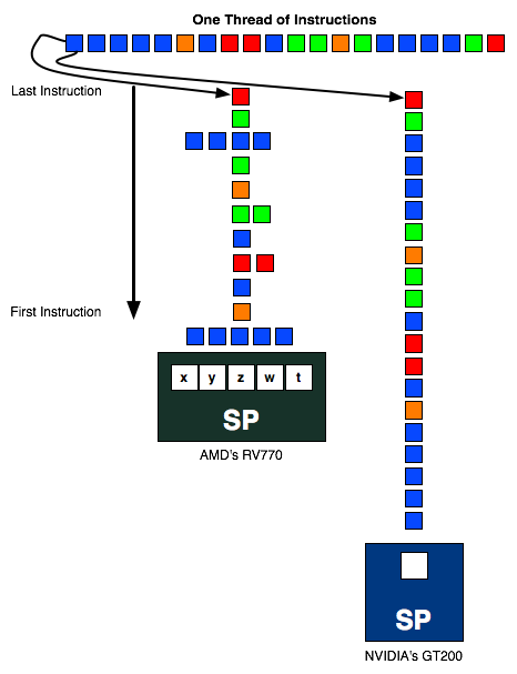
I agree 'scaling' has to take into account many things, for what what AMD lacks in the geometry pipeline they can make up for in compute (if executed well). Here's an example from AT's 4870 review:

ilp.png

Optimally AMD can execute one instruction 5 times quicker than Nvidia, but thats purely theoretical, in practice it may work out to be twice the speed.

As usual, the conclusion really depends on what application we are using to determine 'scaling'. But in general I'd say Fermi has a better chance of a stable increase in performance across the board (I won't say linear) with increased Corespeed whereas AMD can have huge benefits also but it has to be coded right- if not, theres still performance to gain but not as much comparatively speaking.
 

extra

Golden Member
Dec 18, 1999
1,947
7
81


But yeah, card with the highest fillrate being the fastest is merely coincidental here, as a theoretical Fermi dual chip card (assuming it's even possible to dissipate that much power in such a small area) would be king with lower fillrate.


This is all just speculation really but meh ;)

I do think that fill rate is important. Those that can afford a $400-600 video card are very likely to also be able to afford one of the highest rez displays, so that really weighs heavily, imho, in favor of the 5970 if you are going to go ahead and spend that much anyway.

But it's not like fermi has a BAD fill rate. It's good, just not AS good. That's like saying the 5xxx series has a crappy tessellator. That'd obviously be a 'tarded comment. It's still good at games, Fermi just is faster at tessellation. It's obvious that Nvidia had to make trade-offs. So did ATI, which you can read about in that great article about showing up to the fight that anand posted...I'd argue that for most gamers this time around ATI is the better choice. I think ATI "won" this round for the gaming and enthusiast market. But the future, who knows. Fermi isn't another FX series. FX was hot, loud, and slow. Fermi is hot, loud, and fast.

The thing I asked earlier no one really answered...is it possible that a cut down fermi part may not lose as much fill rate, proportionally, as you'd expect? If so, that could be a very good thing. I'm curious to see what Nvidia's $200 dx11 part will look like, assuming it comes out anytime soon.

I get the feeling though that ATI could lower the crap out of their prices any time they wanted, and we are just getting gouged because they can (not that that's bad, company needs to make a profit, but I want cheap cards lol).
 

Cookie Monster

Diamond Member
May 7, 2005
5,161
32
86
Surprisingly though, fermi seems to OC rather well from what I have seen so far and the gains are typically bigger than OC'ing cypress, sometimes by quite a lot. Loud and expensive yes, but performance is better than expected.

Because the current GF100 chips use high leakage parts, I think they have quite abit of OC headroom. But because they are high leakage parts, they are trading high power consumption due to those leaks for higher clock frequencies. Im not sure whether its a linear relationship or not but this can explain why they consume so much power, yet they have a decent OC headroom. Remember those TWKR chips from AMD? they were high leakage parts, guaranteed for very high OC numbers.

Heat also causes higher power consumption figure and I remember reading from a post from Dave Baumann, where he said that 1C roughly equaled to 1W on cypress parts. This means that with adequate cooling, the current GF100 incantations could possibly draw less power than what we are seeing in reviews (although this is assuming 1W = 1C it could be lower or higher).
 
Last edited:

dug777

Lifer
Oct 13, 2004
24,778
4
0
My speculation as to the slower RV870 performance almost regardless of memory clocks is slightly different. I vaugely recall at some stage in an article Anand did that he mentioned some stuff had to be cut out to make the chip a certain target size, and one of the things I recall him mentioning was memory controller related transistors...hence my working theory is that the actual hardware on die that handles memory interaction is physically I/O limited well before the sort of clock rates GDDR5 is capable of...

Hmm, here we go:

In order to run the GDDR5 memory at the sort of data rates that ATI was targeting for the 5870 the analog PHYs on the chip had to grow considerably. At 16mm on a side ATI would either have to scale back memory bandwidth or eat into the shader core area. Either way we would’ve had a slower chip.

Not quite what I recall, but if you squint a bit you can arguably imply my theory from that (in that they cut it down from 22mm to 18mm, and Anand does not say that memory bandwidth was not affected in that cut, or that ATI hit the data rates (note he said data rates not clock rates as well) they wanted initially), and it would explain the results people see from the massive memory overclocks that 5770s in particular are capable of...I don't know that I have ever been fully convinced of the 'magical ECC' argument in that regard, I find it easier to believe that the GDDR5 is physically capable of getting up to those kinds of speeds without throwing errors but the chip can't make use of that...

My 2c :)
 
Last edited:

BFG10K

Lifer
Aug 14, 2000
22,709
2,958
126
Which is obvious in the numbers we have seen- clearly it bests the 285 and even the 295, but that isn't what it has to compete with. The close to linear drop off based on pixel requirements is more then a bit odd(36%, 36%, 37%, 34% on the games I checked on AT moving from 19x12 to 25x16).
You’re assuming the drop is based on texture fillrate, which hasn’t been proven to be the case. Also the latest word is that 2560x1600 performance will be addressed in a future driver.

A game that is heavily shader bound on one of the other parts could very easily be nigh entirely texel bound on the Fermi parts.
Then it’d also be bound the same way on GT200 parts given they have less effective texturing performance, but that hasn’t been the case.

That is a huge reworking of the die for relatively small die space gains, it also destroys their design philosophy in terms of binning. I understand where you are coming from, but a more realistic angle would have been to cut the shader hardware in ~half. Based on current games, that seems about where it should be to match up with what we currently consider balanced.
You can’t cut the shader hardware in half, not without reducing texturing and geometry performance by the same amount, given those units are tied to the SMs.

The idea here is to remove parts of the chip not needed by gamers and producing a “gamer edition” of the card. With such a massive transistor count compared to the 5xxx parts, there must be much more than DP that could be removed without altering gaming performance.

But their higher end parts do, and the GeForce is going to be used in certain worksation applications(CS5 as a general example).
99.99% of gamers won’t be running CS5.
 

sxr7171

Diamond Member
Jun 21, 2002
5,079
40
91
The fact that PC Video cards are so much more powerful than the Console GPUs is probably part of the problem.

1080p is becoming the standard in LCD TVs these days.

This begs the question: Why do PC video cards need to be so much more powerful than a Console? Are 2560x1600 LCD users the only ones who will want a discrete card?

The vast majority of Xbox games are rendered at 720p. That's a huge difference in number of pixels.
 

BFG10K

Lifer
Aug 14, 2000
22,709
2,958
126
Again FILLRATE is still king.

3dm-texture.gif

So is a 5830 is faster than the GTX480 based on your graph? And the 5770 is equal to a GTX470?

Not only are synthetic benchmarks totally useless for real world performance, this one is even more useless because it doesn't even test texturing performance properly. From your own link:

We learned in the process of putting together our Radeon HD 5830 review that 3DMark's texture fill rate test really is just that and nothing more—textures aren't even sampled bilinearly.

Do you play games using point filtering?

58xx has more texture fillrate. GF100 has much more Pixel fillrate and bandwidth though. Now if GF100 had less pixel and bandwidth guess which one would be the clear victor?
Are you talking about theoretical specs, or your graphs? Because based on the pixel fillrate graph on the same page...

3dm-color.gif


...is a GTX260 equal to a GTX470, and a GTX285 faster than a 5870?

Clearly both graphs are absolutely nonsensical from a real world performance point of view, and inferring "fillrate is king" from them is equally nonsensical.

Now, if you're talking about theoretical specs, well, the GTX470 has much less texturing and bandwidth and only a little more pixel fill than a GTX285, but it's 30%-45% faster with 4xAA/8xAA overall: http://www.computerbase.de/artikel/...470/18/#abschnitt_performancerating_qualitaet

Likewise, the 5770 has much less bandwidth, pixel and texel fillrate than the GTX260, yet it's an approximate equal in real world performance.
 
Last edited:

Fox5

Diamond Member
Jan 31, 2005
5,957
7
81
Heat also causes higher power consumption figure and I remember reading from a post from Dave Baumann, where he said that 1C roughly equaled to 1W on cypress parts. This means that with adequate cooling, the current GF100 incantations could possibly draw less power than what we are seeing in reviews (although this is assuming 1W = 1C it could be lower or higher).

Logic fail, correlation != causation. Better cooling shouldn't lower the power consumption of fermi. Well, maybe super cooling it would, but I don't think air or water cooling would have a noticeable effect.

Also, Fermi might just scale better than Cypress because:
1. It has more bandwidth. Cypress hits a bottleneck sooner.
2. The percentage overclocks are bigger. A 200Mhz overclock on Fermi is a bigger percentage than a 200Mhz overclock on Cypress.

The vast majority of Xbox games are rendered at 720p. That's a huge difference in number of pixels.

Many are rendered under that and upscaled. Halo 3 is practically SD resolution. There was talk that the xbox 360 was originally designed primarily as an SD system, upscaling HD for the few who had HDTVs, but HDTV took off faster than expected. (when design started, HDTVs were almost unheard of)
 

AzN

Banned
Nov 26, 2001
4,112
2
0
So is a 5830 is faster than the GTX480 based on your graph? And the 5770 is equal to a GTX470?

Not only are synthetic benchmarks totally useless for real world performance, this one is even more useless because it doesn't even test texturing performance properly. From your own link:

We learned in the process of putting together our Radeon HD 5830 review that 3DMark's texture fill rate test really is just that and nothing more—textures aren't even sampled bilinearly.

Do you play games using point filtering?

Did you forget to read the responses between archangel? Texture is only part of the equated fillrate. Bandwidth and pixel is part of that equation which GTX 4xx is stronger.

And for you info that graph is showing FP16 blending tests which makes sense more modern games instead of 3dmark 2k6 that tests bi linearly for older games.

Are you talking about theoretical specs, or your graphs? Because based on the pixel fillrate graph on the same page...

3dm-color.gif


...is a GTX260 equal to a GTX470, and a GTX285 faster than a 5870?

Clearly both graphs are absolutely nonsensical from a real world performance point of view, and inferring "fillrate is king" from them is equally nonsensical.

Now, if you're talking about theoretical specs, well, the GTX470 has much less texturing and bandwidth and only a little more pixel fill than a GTX285, but it's 30%-45% faster with 4xAA/8xAA overall: http://www.computerbase.de/artikel/...470/18/#abschnitt_performancerating_qualitaet

Likewise, the 5770 has much less bandwidth, pixel and texel fillrate than the GTX260, yet it's an approximate equal in real world performance.
Nonsense to you maybe. Again 3dmark is a tool to test different parts of video cards. Just because you can't consume the information does not mean it's useless. Many quality hardware sites use it as a tool much like a gaming benchmark.

5770 has a whole lot more texture fillrate with FP16 blending. That's why it does so well in modern games while older cards like GTX 260 crushes 5770 in older games.

Tell me BFG what happened when you overclocked your GTX285 core clocks, SP, and memory? Which made the most impact in games? I rest my case. Fillrate is still king long as it's not constraint by bandwidth or shaders.

Now that your case is at rest, let this be as confrontational as you plan on getting in the thread. Anything more than this and you're out. This is not a contest of who is right and who is wrong. This goes for everyone. It's a technical discussion about GPU architecture. End this now.

Anandtech Moderator - Keysplayr
 
Last edited by a moderator:

ArchAngel777

Diamond Member
Dec 24, 2000
5,223
61
91
Heat also causes higher power consumption figure and I remember reading from a post from Dave Baumann, where he said that 1C roughly equaled to 1W on cypress parts. This means that with adequate cooling, the current GF100 incantations could possibly draw less power than what we are seeing in reviews (although this is assuming 1W = 1C it could be lower or higher).

Although this *might* be technically correct, but remember that the only way to reduce the chip temperature is to lower the ambients, increase airflow or a combination of the two. Or you could get into exotic cooling, but I won't go there with this post. Lets take the most common approach 'fan speed'. The fan can only be so large on a practical level, so the only way to increase heat dissipation is to increase the fan speed, this in turn requires more power to the fans. So, you don't really lower power consumption overall.
 

HurleyBird

Platinum Member
Apr 22, 2003
2,684
1,267
136
Then it’d also be bound the same way on GT200 parts given they have less effective texturing performance, but that hasn’t been the case.

Actually, the real world data implies that Nvidia might not have been entirely forthright when they told everyone that despite the theoretical handicap Fermi has more texturing performance than GT200.

http://www.computerbase.de/artikel/...geforce_gtx_480/5/#abschnitt_skalierungstests

All of the scaling tests are interesting, but pay close attention to the AF tests. GT200 has the best scaling, Cypress is right behind, but Fermi starts to develop a real performance deficit in two of the three games tested.
 

cbn

Lifer
Mar 27, 2009
12,968
221
106
Does anyone here see Fermi as being a capable chip for Shared frame rendering?

Could Nvidia actually reduce input lag and increase FPS (in an efficient way) using this method? Maybe a Co-op type Video card where the small GPU does all the easier tasks and the Large GPU works on the parts of the frame bottlenecking the processing time?
 
Last edited:

Cookie Monster

Diamond Member
May 7, 2005
5,161
32
86
Logic fail, correlation != causation. Better cooling shouldn't lower the power consumption of fermi. Well, maybe super cooling it would, but I don't think air or water cooling would have a noticeable effect.

Also, Fermi might just scale better than Cypress because:
1. It has more bandwidth. Cypress hits a bottleneck sooner.
2. The percentage overclocks are bigger. A 200Mhz overclock on Fermi is a bigger percentage than a 200Mhz overclock on Cypress.

Theoretically it does. All electronic components do, though it really depends on the material used.

Quotes from my source ala B3D :
aaronspink said:
yes. Most likely you would have a measurable difference in power from a ~20c operating differential.

Mintmaster said:
Joking aside, higher temperatures should affect leakage. Undoped Si between transistors, p-n junctions, and even the gate insulator increases in conductivity, and higher temperature increases tunnelling current, too. I don't think the resistance of the doped areas make much difference to power consumption.

SiliconAbyss said:
But I did several tests on my Cypress when First got my card and I can confirm that what Dave said is very correct. +1C=+1W at full load for stock HD5870 between 70C and 85C at least.

Heres an example of a GTX280 consuming diff power consumption figures as load temps change

Link

edit - So what this suggests is that with a better cooling, one could shave 10~30W or maybe more during load depending on how low the temperature is. Maybe someone with a GTX480/470 can test this theory out. (Killawatt method wont work since that involves losses from other factors as its measuring directly from the AC source.)
 
Last edited:

HurleyBird

Platinum Member
Apr 22, 2003
2,684
1,267
136
Thanks cookie monster, that's really cool. Makes perfect sense but I never realized computer chips worked that way in regards to power consumption until now.
 
Last edited:

ArchAngel777

Diamond Member
Dec 24, 2000
5,223
61
91
Theoretically it does. All electronic components do, though it really depends on the material used.

Quotes from my source ala B3D :


Heres an example of a GTX280 consuming diff power consumption figures as load temps change

Link

edit - So what this suggests is that with a better cooling, one could shave 10~30W or maybe more during load depending on how low the temperature is. Maybe someone with a GTX480/470 can test this theory out. (Killawatt method wont work since that involves losses from other factors as its measuring directly from the AC source.)

This is VERY interesting... Thanks for posting.