Discussion Apple Silicon SoC thread

Page 325 - Seeking answers? Join the AnandTech community: where nearly half-a-million members share solutions and discuss the latest tech.

Eug

Lifer
Mar 11, 2000
23,780
1,351
126
M1
5 nm
Unified memory architecture - LP-DDR4
16 billion transistors

8-core CPU

4 high-performance cores
192 KB instruction cache
128 KB data cache
Shared 12 MB L2 cache

4 high-efficiency cores
128 KB instruction cache
64 KB data cache
Shared 4 MB L2 cache
(Apple claims the 4 high-effiency cores alone perform like a dual-core Intel MacBook Air)

8-core iGPU (but there is a 7-core variant, likely with one inactive core)
128 execution units
Up to 24576 concurrent threads
2.6 Teraflops
82 Gigatexels/s
41 gigapixels/s

16-core neural engine
Secure Enclave
USB 4

Products:
$999 ($899 edu) 13" MacBook Air (fanless) - 18 hour video playback battery life
$699 Mac mini (with fan)
$1299 ($1199 edu) 13" MacBook Pro (with fan) - 20 hour video playback battery life

Memory options 8 GB and 16 GB. No 32 GB option (unless you go Intel).

It should be noted that the M1 chip in these three Macs is the same (aside from GPU core number). Basically, Apple is taking the same approach which these chips as they do the iPhones and iPads. Just one SKU (excluding the X variants), which is the same across all iDevices (aside from maybe slight clock speed differences occasionally).

EDIT:

Screen-Shot-2021-10-18-at-1.20.47-PM.jpg

M1 Pro 8-core CPU (6+2), 14-core GPU
M1 Pro 10-core CPU (8+2), 14-core GPU
M1 Pro 10-core CPU (8+2), 16-core GPU
M1 Max 10-core CPU (8+2), 24-core GPU
M1 Max 10-core CPU (8+2), 32-core GPU

M1 Pro and M1 Max discussion here:


M1 Ultra discussion here:


M2 discussion here:


Second Generation 5 nm
Unified memory architecture - LPDDR5, up to 24 GB and 100 GB/s
20 billion transistors

8-core CPU

4 high-performance cores
192 KB instruction cache
128 KB data cache
Shared 16 MB L2 cache

4 high-efficiency cores
128 KB instruction cache
64 KB data cache
Shared 4 MB L2 cache

10-core iGPU (but there is an 8-core variant)
3.6 Teraflops

16-core neural engine
Secure Enclave
USB 4

Hardware acceleration for 8K h.264, h.264, ProRes

M3 Family discussion here:


M4 Family discussion here:

 
Last edited:

FlameTail

Diamond Member
Dec 15, 2021
3,709
2,156
106
Apple A18 chip rumours:
GV8vmS7XgAAaHyd.jpeg
GV8vmRabUAALJcw.jpeg
I presume the notation stands for "CPU P-cores + CPU E-cores + GPU cores".

So the A18 Pro gets one extra GPU core.

Take this rumour with a large grain of salt though, because apparently this is not a very reliable leaker.
 

jdubs03

Senior member
Oct 1, 2013
593
220
116
Feels like that’s not enough differentiation. But if so tbh I’d be surprised if the standard 16s didn’t sell a lot better than the standard 15s. The 16s are going to see such an upgrade relative to the Pros.
 

poke01

Golden Member
Mar 8, 2022
1,952
2,479
106
Apple A18 chip rumours:
View attachment 106296
View attachment 106297
I presume the notation stands for "CPU P-cores + CPU E-cores + GPU cores".

So the A18 Pro gets one extra GPU core.

Take this rumour with a large grain of salt though, because apparently this is not a very reliable leaker.
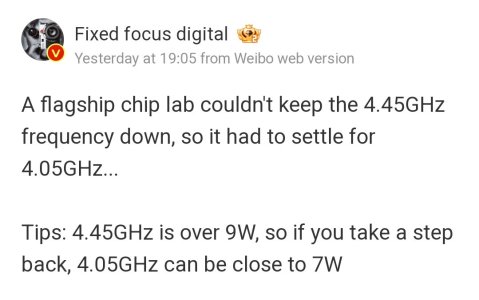
I doubt A18 was ever going to be 4.45GHz anyway, that’s M4 clocks. I don’t think the A series ever matched the M series in clocks.
 

FlameTail

Diamond Member
Dec 15, 2021
3,709
2,156
106
I doubt A18 was ever going to be 4.45GHz anyway, that’s M4 clocks. I don’t think the A series ever matched the M series in clocks.
If the rumours of the Snapdragon 8 Gen 4 coming in at 4.47 GHz are true, then for the first time in many years, Apple will surrender the smartphone SoC clock speed crown to Qualcomm.

Not that it matters really. Absolute performance, IPC and Performance-per-watt are more important metrics.
 
Last edited:
  • Like
Reactions: Mopetar and poke01

mvprod123

Junior Member
Jun 22, 2024
12
6
41
Apple A18 chip rumours:
View attachment 106296
View attachment 106297
I presume the notation stands for "CPU P-cores + CPU E-cores + GPU cores".

So the A18 Pro gets one extra GPU core.

Take this rumour with a large grain of salt though, because apparently this is not a very reliable leaker.
Hmm, the 2+4 configuration again. After the M4 release, I was expecting +2 additional e-cores. Perhaps Apple will introduce a new architecture for E-core in A18? I wonder if the A18 will bring a new GPU architecture.
 

jdubs03

Senior member
Oct 1, 2013
593
220
116
Hmm, the 2+4 configuration again. After the M4 release, I was expecting +2 additional e-cores. Perhaps Apple will introduce a new architecture for E-core in A18? I wonder if the A18 will bring a new GPU architecture.
There had been chatter in this thread I think a few months ago that posited a new E-core microarchitecture. They have to do some sort of a bump because at least in MT both Mediatek and the S8G4 are going to provide a challenge.
 

mvprod123

Junior Member
Jun 22, 2024
12
6
41
If the rumours of the Snapdragon 8 Gen 4 coming in at 4.47 GHz are true, then for the first time in many years, Apple will surrender the smartphone SoC clock speed crown to Qualcomm.

Not that it matters really. Absolute performance, IPC and Performance-per-watt are more important metrics.
Oryon tries to compensate for the lag in IPC with a higher clock speed.
 

Doug S

Platinum Member
Feb 8, 2020
2,678
4,528
136
I doubt A18 was ever going to be 4.45GHz anyway, that’s M4 clocks. I don’t think the A series ever matched the M series in clocks.

Yeah they've always been 10% lower so 4.0 or a little higher is where I had guessed A18P clocks would end up. Gotta live how they try to make it sound like someone screwed up and they had to cut the clock rate, rather than just stating this is business as usual...

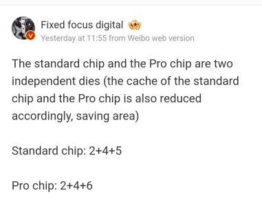
I don't get the claims around the two different dies though, especially if the only difference is one GPU core and a bit of SLC. You'd think there would have to be additional differences like bigger NPU and maybe wider memory path to generate enough area savings to be worth taping out separate designs.
 

Doug S

Platinum Member
Feb 8, 2020
2,678
4,528
136
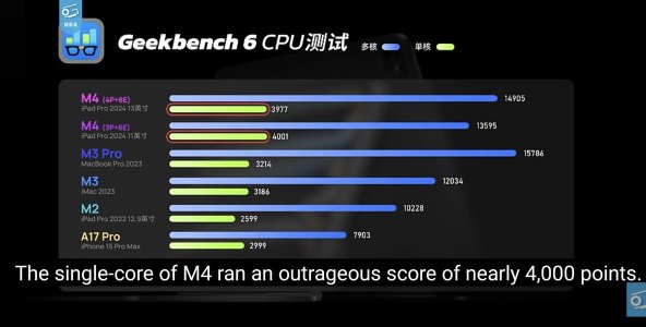
That's with liquid nitrogen.

So?

Active cooling should easily dissipate the heat from a SINGLE CORE and allow it to match LN2 results of the iPad Pro.

I think people are mentally equating that test to what extreme overclockers using LN2 do on a PC, but the M4 wasn't overclocked. It was just prevented from having to throttle its frequency because as installed in an iPad Pro it is not actively cooled and even a single core running at a single digit number of watts puts out more heat than a 5.1mm form factor is able to passively radiate to the surrounding environment. Even the puny heatsink and fan in a Macbook Pro might be enough to avoid throttling, but if not the one in the Mini, Studio and Pro will.

Even with that cooling it sounds like it took a fair number of runs before GB6's innate variability gave Geekerwan the 4000 he was shooting for, so I imagine most results of the M4 in actively cooled Macs will fall a bit short. But there will be runs that hit 4000, there is nothing magic about LN2 that makes it better able to cool a CPU with all of 9 watts coursing through it.
 

naukkis

Senior member
Jun 5, 2002
853
726
136
Wait... what? isn't the current generation having L3 cache and now remove it?
Why this so AMD Carrizo's times?
Per core sliced L3 with fast interconnect is easy way to boost performance but it's also very power inefficient. Intel did also remove it from their efficiency cores and sure will need to remove it from their p-cores too pretty soon if they want to be competitive on efficiency race.
 

FlameTail

Diamond Member
Dec 15, 2021
3,709
2,156
106
Per core sliced L3 with fast interconnect is easy way to boost performance but it's also very power inefficient. Intel did also remove it from their efficiency cores and sure will need to remove it from their p-cores too pretty soon if they want to be competitive on efficiency race.
ARM Cortex cores also have an L3. Would you say the same for them?
 

naukkis

Senior member
Jun 5, 2002
853
726
136
ARM Cortex cores also have an L3. Would you say the same for them?
It does have one unified L3 like AMD phenom did in past. It ain't well performing solution - path forward is either slice L3 per core or use large L2 instead. Large L2 serving multiple cores seems to be best perf/watt for mobile.
 

FlameTail

Diamond Member
Dec 15, 2021
3,709
2,156
106
It does have one unified L3 like AMD phenom did in past. It ain't well performing solution - path forward is either slice L3 per core or use large L2 instead. Large L2 serving multiple cores seems to be best perf/watt for mobile.
Oh, so there is distinction- Unified L3 vs Sliced L3.

Is the large L2 used in Apple or Qualcomm Oryon CPUs Unified or Sliced?
 

naukkis

Senior member
Jun 5, 2002
853
726
136
Oh, so there is distinction- Unified L3 vs Sliced L3.

Is the large L2 used in Apple or Qualcomm Oryon CPUs Unified or Sliced?
Unified. Sliced cache is unsuitable for low power because one active core keep all slices and interconnect powered. Unified cache instead can power off unused parts even when servicing active core.
 
  • Like
Reactions: FlameTail

name99

Senior member
Sep 11, 2010
483
364
136
Wait... what? isn't the current generation having L3 cache and now remove it?
Why this so AMD Carrizo's times?
What is the purpose of an L3? remember that these designs (both Apple and QC) are not clones ofx86 designs from the 90s.

1) L3 acts as a LARGE cache. This was important back when process was very different, and the mantra was that L1 is optimized for latency, L2 is optimized for bandwidth, L3 is optimized for capacity. But time moves on, and nowadays Apple and QC are both able to provide very impressively sized L2's (eg 12 or 16MB), so this is not an important issue.

2) L3 acts as a mechanism of COMMUNICATION. This is important, but again for Apple and QC it's handled by the SLC (System Level Cache). The SLC can be called an L3, but to do so shows that you really don't understand what's going on. SLC is NOT optimized for capacity, like an L3, it's optimized for communication and issues related to that.
One aspect of this is that a good SLC is a memory-side cache, meaning that the memory controller is aware of what's in the cache. This in turn means that IP blocks that are "not coherent", that is they don't take part in cache snooping, can still transfer data through the SLC, they don't have to write that data to DRAM.
A second aspect is that there's usually a lot of control over details of the SLC to ensure that various communicating clients (eg camera streaming data to video compression block via SLC) get the performance they need. At the simplest level this is per-client quotas, but Apple gets MUCH more elaborate (data set IDs that allow different data streams not to interfere with each other, various levels of cache persistence, QoS levels, etc). QC probably copy much of this, but I don't know.

3) So we have seen that Apple and QC handle Capacity via large L2, and Communication via SLC. There is one more theoretically interesting use case for L3, namely cache compression.

The simplest cache compression is a zero-content cache, which adds a side cache that contains only address tags and line flags, not data, to hold lines that are all zeros. This is worth doing because a shockingly large number of lines are only zeros. This is easily enough added to the side of an L2 or even L1, and doing so is basically an issue of "do we have the engineering time to do it, and what do simulations show as the best capacity/energy/area tradeoffs". I'm unaware of any commercial implementation so far, but my GUESS is we will see this soon on Apple just as a consequence of the lack of scaling of SRAM - zero-content cache is a nice way to trade off logic against SRAM: make the L1D and/or L2 caches look 10 to 20% larger by adding more logic but not much more SRAM.

But "real" cache compression hopes to compress more generic lines, and succeeds a surprisingly large fraction of the time, generally packing two lines into one. (You can go further, but that seems impractical, at least for now). This is nice in terms of getting say 1.5x capacity at the cost of some extra logic --- but ALSO at the cost of some extra latency. Which is negligible in the context of L3 latencies, but more visible in terms of L2 latencies. So that rather throws a spanner in the works...
What to do?

Obviously I have no idea what Apple's plans are, but options might include
- implement DRAM compression rather than L3 compression. (Note this is a light compression that packs many, not all, "cache lines pairs" into a single cache line in DRAM. It's not to be confused with page compression, which is much more aggressive -- and much much slower.)
This gives you a capacity win for your DRAM, something that doubtless appeals to Apple; and a power win (since one DRAM access gives you twice as much data). OTOH it's not worth doing if MOST of the data in DRAM turns out to be already compress (eg compressed images, text, video, machine models, etc). I don't know if Apple will see it as worth doing.
QC implemented this for Centriq, so it's certainly doable and practical; but Centriq targeted a different market.

- shrink the size of the per-cluster L2 and add a system-wide L3 that serves the CPU clusters (maybe also the GPU?), and that is lower latency but supports compression? Differs from the SLC in that it's NOT set up for all the communication tasks I described.
 

name99

Senior member
Sep 11, 2010
483
364
136
It does have one unified L3 like AMD phenom did in past. It ain't well performing solution - path forward is either slice L3 per core or use large L2 instead. Large L2 serving multiple cores seems to be best perf/watt for mobile.
Oh there are many additional ways to slice this.

Yet another option is Virtual L3. This is what IBM does on its newest mainframes. Essentially each core has a huge (like 36MB) L2, but the L2's are all connected together (not just by wires, but with a fancy protocol that's more sophisticated than basic MESIF/MERSI) so that a core can read from the L2 of another core, fulfilling the roles of L3 (capacity and communication).

Apple does a weak version of this (or at least they have a patent to do so, and all the tech in place). The SLC has tags that cover every lower cache in the system so the SLC has tags that cover, eg the cache used by the media block. This means that data can be stored in the media block visible to the SLC, when the media block is not in use, extending the capacity of the SLC...
 
  • Like
Reactions: Mopetar and Tlh97