People are being anal and smartass about what big.LITTLE actually means - there are those that seem to say that it's ARM's specific implementation of heterogeneous CPU cores consisting of separate independent CPU clusters interconnected through a coherent interconnect fabric.
To
me (just my and other's subjective opinion) big.LITTLE means nothing more than the use of heterogeneous CPU cores in a system for the sake of power or performance optimisation. That's what "big.LITTLE" has become in lay-man terms.
Because I don't want to get into useless arguments with you because it's a futile exercise, but I will indulge you on the current topic just because of how stupid it is.
Are you really now trying to use wording semantics to prove a technical point? Can we stop this nonsense?
https://github.com/AndreiLux/ref-3.10/blob/perseus7420/drivers/bts/bts-exynos7420.c
Code:
#define MIF_BLK_NUM        4
....
    __raw_writel(exynos7_bts_param_table[target_idx][BTS_MIF_DISP + rot], base_drex[0] + QOS_TIMEOUT_0xB);
    __raw_writel(exynos7_bts_param_table[target_idx][BTS_MIF_DISP + rot], base_drex[1] + QOS_TIMEOUT_0xB);
    __raw_writel(exynos7_bts_param_table[target_idx][BTS_MIF_DISP + rot], base_drex[2] + QOS_TIMEOUT_0xB);
    __raw_writel(exynos7_bts_param_table[target_idx][BTS_MIF_DISP + rot], base_drex[3] + QOS_TIMEOUT_0xB);
....
#define EXYNOS7_PA_DREX0    0x10800000
#define EXYNOS7_PA_DREX1    0x10900000
#define EXYNOS7_PA_DREX2    0x10A00000
#define EXYNOS7_PA_DREX3    0x10B00000
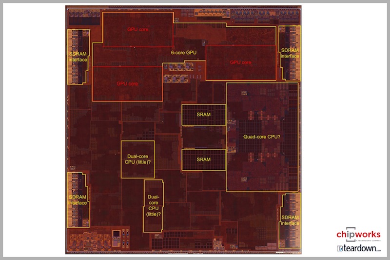
The above is taken from the Bus Traffic Shaper driver of the 7420 as you're talking about that SoC in particular.
Those are just a few excerpts of the hundreds of code pieces pointing out that the "memory controller" beyond having 4 channels also has 4 schedulers (because we're settings different QoS parameters to each "controller's" base address), physical interface (die shot), independent power management, internal clock planes.
To me that looks like 4 "memory controllers", but you're always welcome to provide technical expertise of your own.
How does the S820 matching the A10's Stream numbers in any way suggest to you a single memory controller? How do you even come to this conclusion? Stream performance is mainly dictated by the CPU's memory subsystem. This is why you see ARM boasting about new microarchitectures improving in that regard, this is why you see Samsung boasting their microarchitecture is very good in memory performance. So I ask you again, how do you come to the conclusion that the memory controller is here to either blame or to credit?
What GB multi results are only 2.3x? Where do you even get this number from?
Let me do the job for you:
It's obvious that you're not talking about the E8890 Note 7 as that one's score ratio is far above "2.3x", so let's look at the S820 numbers. Seems fine to me? Do you forget that this SoC has 2 cores at 2150 MHz while the other 2 run up to only 1559 MHz? That's only a theoretical multicore peak of 3.45x over single-core. I won't go into more details on why Kryo is just an outright disappointing microarchitecture but you can assume that the rest of the delta between
the actual 2.74x scaling and the theoretical peak of 3.45x can be found in a bunch of reasons such as software scheduling, overhead, or even bottlenecks in the communication between the two clusters and the central bus.
But let's go back, you mentioned the S6 earlier so I included those scores as well. I don't see nothing wrong there. An average of 4.18x scaling from single to multi-core (Don't forget there are small cores, but they're relatively insignificant because of both their performance and GTS scheduling).
The vanilla Exynos 8890 has worse scaling with a figure of 3.65x over single core, but again that's because the SoC boosts up to 2.6GHz for 2 load threads while it remains at 2288MHz for more threads. So I went ahead and included my own S7 with that mechanism turned off so we're always at 2288MHz, and oh look the scaling goes back to 4.23x.
So what about the memory figures? They mean nothing in regards to multi-core performance scaling as evidence by the actual benchmarks here. All it means is that each CPU is powerful enough to saturate a) either the cluster L2 subsystem b) the interconnect bandwidth which we've seen in the past is often much less than total theoretical memory controller
(s) bandwidth.
So again, where is this "pattern among high-end devices?". I don't see it. The last few flagships SoCs sure didn't have it. Are you looking at S810 devices which can't even do full freq for all cores?
David warned you on RWT about people complaining about your discussion tone and I absolutely agree that it's absolutely offputting to even argue with you about anything. You have such a chip on your shoulder against me that you attacked
me in the comments section of the process node pipeline even though I had nothing to do with it and Anton wrote the article. That alone is just enough reason to probably make this the last time I engage with you directly. I see no point in arguing with somebody who thinks he's always correct, got better things to do.