[Anandtech]: GlobalFoundries Stops All 7nm Development !!

Page 12 - Seeking answers? Join the AnandTech community: where nearly half-a-million members share solutions and discuss the latest tech.

CatMerc

Golden Member
Jul 16, 2016
1,114
1,149
136
PC enthusiasts live in a semiconductor bubble. The vast majority of volume isn't made on N nodes. Not even on N-1, or N-2 nodes. Heck we're running out of capacity for 200mm wafers, when was that bleeding edge again?

GloFo will be fine, their FDSOI nodes combined with IBM tech is the best in the industry for RF, and that 400m deal will likely grow with the current administration's China panic. They're going to make bank with the burden of bleeding edge nodes taken off their backs.

I also don't believe they stopped FDSOI node development. 12FDX will likely happen, just not very soon.
 

DrMrLordX

Lifer
Apr 27, 2000
21,617
10,826
136
China panic.

Woops, forgot that part. Anyone with fabs State-side will have a license to print money, for awhile. Heh. Also DoD sourcing, as has been mentioned elsewhere . . .

12FDX will likely happen, just not very soon.

You really think so? That process won't come for free. They're gonna have to earn it the hard way, since cash from the UAE isn't flowing freely now . . .
 

CatMerc

Golden Member
Jul 16, 2016
1,114
1,149
136
Woops, forgot that part. Anyone with fabs State-side will have a license to print money, for awhile. Heh. Also DoD sourcing, as has been mentioned elsewhere . . .


You really think so? That process won't come for free. They're gonna have to earn it the hard way, since cash from the UAE isn't flowing freely now . . .
I doubt the Arabic money stopped flowing entirely. Rather it shrunk and diverted to more profitable possibilities (FDX). They would be dumb to not develop future nodes, their current nodes won't give them return on investment for all the fabs they bought up.

You might say it's sunk cost, but when there's a license to print money, and a clear market opportunity, that's hardly the time to cut your losses and just lose that position. If GF had nothing at all that makes them unique that would be a different story.

Another important factor is that companies look for a roadmap of nodes, not just a single node. Some might just not bother with your node if they can't trust you to keep improving upon the foundation.
 
Last edited:

NostaSeronx

Diamond Member
Sep 18, 2011
3,686
1,221
136
One of the 7nm things that probably went with it?
https://www.rcrwireless.com/2018060...-chips-for-machine-learning-tag41#prettyPhoto
https://ujg433eawlo3i4uqknhm8e1b-wp...t/uploads/2018/06/20180605_134543-702x336.jpg

CPU Cores & L2/L3 Cache to CPU cores on die1 and L2/L3 cache on die2.
=> 60% cost reduction:
- Chip w/ CPU+L2/L3 = $100 arb
- Stacked chip w/ CPU on die 1 and L2/L3 on die 2. = $40 arb

Another is that 7HP was indeed after 14HP:
https://electroiq.com/insights-from...ies-adv-packaging-tends-in-foundry-the-space/
http://electroiq.com/insights-from-leading-edge/wp-content/uploads/sites/4/2018/05/fig-1-2.jpg
HBM2 Flarebolt/Aquabolt(Samsung names for 2 Gbps and 2.4 Gbps models) = 96 mm squared measured
HBM2 PHY is only 12 mm squared.

7nm would have brought 4x HBM (Vega 20) and later on another node 6x HBM?

Also, looking through another slide:
https://www.nextbigfuture.com/2017/03/global-foundries-will-use-free-electron.html
GlobalFoundries N3 node wouldn't have launched till 2023. One year after TSMC, and three years after Samsung.
 
Last edited:

krumme

Diamond Member
Oct 9, 2009
5,952
1,585
136
Woops, forgot that part. Anyone with fabs State-side will have a license to print money, for awhile. Heh. Also DoD sourcing, as has been mentioned elsewhere . . .


You really think so? That process won't come for free. They're gonna have to earn it the hard way, since cash from the UAE isn't flowing freely now . . .
Agree. I missed the chinapart also. Good argument. Its a tangible advantage to have stateside fabs. And it doesnt go away with the current administration and hysteria. I mean anybody on this earth will avoid china to protect their ip and future business.
I can see that as a very solid advantage for gf that they need to use 100%
 

scannall

Golden Member
Jan 1, 2012
1,946
1,638
136
A few thoughts on this. Perhaps not keeping with the rampant speculation that others are posting.

By all indications they were roughly on track to get 7nm up and running. But, to actually fill orders would have involved buying more equipment and expanding a fab. Or building a new one. An investment that they were unwilling to make. That seems more than a little short-sighted to me. Even if in the future they return to developing high end, they won't be trusted. The only thing that gave them any trust and ability in the first place was the IBM deal.

They were essentially given the keys to the kingdom with all those IBM process engineers. Some of the best around. And squandered the opportunity. Perhaps this wil be a good thing for Intel? I'm sure Intel would be happy to pick them up for their own process woes. Apple may scoop some up as well.

Overall it's bad for the industry. Not disastrous by any means. But fewer and fewer points of supply is never a good thing.
 

DrMrLordX

Lifer
Apr 27, 2000
21,617
10,826
136
I doubt the Arabic money stopped flowing entirely. Rather it shrunk and diverted to more profitable possibilities (FDX). They would be dumb to not develop future nodes, their current nodes won't give them return on investment for all the fabs they bought up.

We'll see. I would expect future developments to come slowly. Plus the 12nm node probably has some legs. Hell, the DoD/military contractor world is still stuck on 90nm or larger. If GF can make sales on that (or something else they're still tooled to run) they can sell from those nodes for years. Pretty sure the automotive world would be receptive of older nodes as well.

Another important factor is that companies look for a roadmap of nodes, not just a single node. Some might just not bother with your node if they can't trust you to keep improving upon the foundation.

I guess at this point, the best thing to do would be to compare GF to other semiconductor fabricators who don't push leading-edge nodes anymore. How often do they update their nodes?
 

NostaSeronx

Diamond Member
Sep 18, 2011
3,686
1,221
136
SOITEC & MBDA purchased Dolphin Integrated a 22FDX/FDXcelerator partner. They have also designed on STM's 28FD.

“Dolphin Integration represents a strategic opportunity for Soitec to reinforce a full IP and service offering related to energy efficient solutions for chip design on FD-SOI. This is a major differentiating factor for FD-SOI and a key accelerator of FD-SOI adoption in major market segments,” highlighted Paul Boudre, CEO of Soitec.

“MBDA investment will strengthen the French defense industrial base since it will provide Dolphin Integration with a more stable flow of defense related revenues and a closer technological collaboration that will allow it to enhance the access of its specialized microelectronics offering to the entire French and European defense industry,” said Antoine Bouvier, CEO of MBDA.

MBDA is jointly owned by Airbus (37.5%), BAE Systems (37.5%), and Leonardo (25%).

AirBus seems to be 110nm to 45nm, with works on FD28 via DAHLIA.
BAE 45nm => https://www.baesystems.com/en-us/ou...uct-sites/space-products-and-processing/asics
I'm going to assume Leonardo is the same.
I guess at this point, the best thing to do would be to compare GF to other semiconductor fabricators who don't push leading-edge nodes anymore. How often do they update their nodes?
Based on UMC with comparable technology:
28nm HPM -> 2013
28nm HPC -> 2014
28nm HPCU -> 2016
28nm HPCU+ -> 2H 2017/1H 2018
22nm ULP -> 2H 2018/1H 2019

"Chipmaker UMC expects to introduce 22nm process technology as early as 2018, DigiTimes reports, citing comments made at its investors meeting. The company, which began shipping 14nm chips in Q1, has started IP development for its 22nm process, and plans to introduce the node technology in 2018 or 2019."
- https://thefly.com/landingPageNews.php?id=2542205

"Both 28nm and 22nm process technologies will be the future focus of United Semi, said Chien, adding that the 12-inch foundry is looking to expand its client portfolio and deliver economies of scale as soon as possible.
Monthly production capacity at United Semi is set to reach 25,000 wafers for its first phase of expansion, Chien disclosed.
...
United Semi will build additional production capacity according to customer demand, and will not "blindly" expand capacity, Chien noted."
- http://www.simmtester.com/page/news/printerFormat.asp?num=20185&rnd=163590714670217090
=> Fab 12X maxes at 50,000.

"14nm accounted for 2% of 4Q17 revenue, while 28nm contribution remained at 15%."
https://www.businesswire.com/news/home/20180124005487/en/UMC-Reports-Fourth-Quarter-2017-Results
=> Fab 12X is ramping up.

Most recent:
"Business from 14nm increased to 3% of 2Q18 revenue, while 28nm contribution was 15%."
https://www.businesswire.com/news/home/20180725005300/en/UMC-Reports-Quarter-2018-Results

~1% every two quarters. Hopefully.

28nm ramped up fast:
https://www.eetimes.com/document.asp?doc_id=1326479
1% to 9%...
“A normal ramp would be three to four quarters to get to 20% of revenue, and you’ve already been ramping for four quarters, and it’s only 9% of revenue,” Heyler said."
Normal would be 20%, oof.

So, if revenue was broken down:
"IC Insights, a company that tracks semiconductor data, estimates that GlobalFoundries had $6 billion in revenue in 2017, although it does not break that down in terms of profit."
- https://www.sfchronicle.com/busines...lFoundries-profitable-Yes-and-no-12906650.php

Add that with:
https://www.globalfoundries.com/new...-billion-design-win-revenue-22fdxr-technology
https://www.semiwiki.com/forum/content/7604-fdsoi-status-roadmap.html

One sixth of their revenue was from 22FDX which is 16% of the revenue being FDSOI. 22FDX began in Q1 2017(Validated: Ramp2HVM 2H 2017) and by Q2 2018 had $2 billion USD. So, this year should be $7 billion in revenue. $1 billion in the first half and $1 billion in the second half with pessimistic results.

22FDX is aggressively following historic trends. Which 28nm and 14nm at UMC did not even though they had DDC a competitor of FDSOI on 28nm.

"TSMC is expected to have almost 6x the sales volume at <40nm as compared to GlobalFoundries in 2016 ($15.6 billion for TSMC and $2.6 billion for GlobalFoundries)."
https://electroiq.com/2016/09/leading-edge-leads-the-way-in-pure-play-foundry-growth/

22FDX is basically on par with the entirety of <40nm from 2016 within four quarters. Competition hasn't really even started yet either:
- 22nm ultra-low power (22ULP) technology was developed based on TSMC’s industry-leading 28nm technology and is expected to start production in the second half of 2018.
- 22ULL technology targets the IoT and wearable devices applications and is expected to start risk production in the second half of 2018.

That is with SOITEC B2 @ 100K per year.
PDSOI(also 3D-FD) is being swapped to FDSOI for 350K(400K) wafers per year (2018 -> 2019).
By 2020, the facility will be 800K w/ 650K for 2D-FD and 150K for other.
"Consequently, Soitec expects its Bernin II production site to reach a capacity utilization rate close to 100% towards the end of FY'19 or the beginning of FY'20."
Singapore will qualify in 1H 2019, then by 2H 2019/2020 will also have 800K wafers per year.
There is also plans for a third plant with 1M per year.

8000 wpm (now) -> 33,000 wpm (later1) -> 54,000 wpm (later2)
If demand keeps up would the $2B become <$8B at later1 and <$13B at later2. Then, there is 12FDX which would be a higher revenue source in late 2020 to early 2021. This is ignoring GF Chengdu and SOITEC Singapore, and if GF's Singapore and Malta jump in. Also ignoring extended SOITEC sources/licensees like SEH and GlobalWafers.
 
Last edited:

NostaSeronx

Diamond Member
Sep 18, 2011
3,686
1,221
136
https://nepp.nasa.gov/workshops/etw... 2.5&3D Packaging Status Update 6-19-2018.pdf
June 19, 2018 => Advanced Si Packaging Update
SRAM was 4-high!
HBM support for 8H.

From a PDF of SOITEC: soitec-ddr-2017-2018-vafinale // Company = SOITEC
Related Party Transactions:
Douglas Dunn:
Director of the Company
Director of GF

1- With GLOBALFOUNDRIES U.S., Inc. (GF)
"In April 2017, following authorization from the Board of Directors on March 30th, 2017, your Company signed a contract with GF entitled « Materials Supply Agreement » (« MSA ») with effect from April 25th, 2017.
The MSA defines the general conditions for the purchase of the Company’s products by GF and some of its subsidiaries. In return, the latter undertakes to supply these products, which are identified in the purchase orders or the Addenda attached to the MSA.
This contract is applicable for five years (until March 31st, 2022) and is automatically renewed each year if it is not specifically terminated.
This contract also stipulates the terms for delivery, storage, warranty period and the responsibilities of both parties."

2- With GLOBALFOUNDRIES Dresden Module One LLC &Co. KG (GF Dresden):
"In April and May 2017, following authorization from the Board of Directors on March 30th, 2017, your Company signed a contract with GF Dresden entitled « Product Purchase Agreement » (« PPA »), attached as an appendix to the « Materials Supply Agreement » (« MSA »).
This is an addendum to the MSA that defines the terms and conditions for the consignment of certain products purchased only by GF Dresden. The MSA is thus applicable to the PPA.
This agreement lists the products that will be purchased from the Company by GF Dresden as a consignment sale. The Dresden consignment-specific rules are also defined therein.
The PPA lists the products that will be purchased from your Company by GF Dresden in the context of consignment sales. It also sets out the specific terms applicable to such consignment sales."

3- With GLOBALFOUNDRIES U.S., Inc. (GF):
"In September 2017, following authorization from the Board of Directors on March 30th, 2017, your Company signed a contract with GF entitled « Long Term Addendum to Materials Supply Agreement » (« LTA »), applied retrospectively with effect from July 1st, 2017.
This contract is applicable for five years and is automatically renewed each year if it is not specifically terminated.
The LTA is governed by the rules set out in the « Materials Supply Agreement ».
The LTA specifies the terms under which the Company may meet a major portion of GF and its subsidiaries’ FD-SOI requirements.
The price depends on the volumes purchased and the product yield. They may also change favorably, if GF reduces the cost of acquisition of some of the equipment that is necessary for manufacturing the products. (or) The prices depend on quantities purchased and the efficiency of the products. Prices may also decrease if GF enables a reduction in the acquisition costs of certain equipment used to manufacture the products.
The price of raw materials has no impact on the prices granted to GF.
This contract also stipulates the delivery terms and rules for consignment goods."

4-
With regards to the agreements referred to in points ... above, we inform you that the sales of wafers by the Company to GLOBALFOUNDRIES totaled $74,300,000 during the 2017-2018 fiscal year.
----
<150,000 wafers?
 

catonkatonk

Junior Member
Sep 7, 2018
4
2
41
And after 10nm, how are Intel doing with EUV?

This news just makes me wonder if Intel are wishing that they spun off their fab business.
Which would have been a totally absurd and inconceivable thing to think even, say, two years back.
 

DrMrLordX

Lifer
Apr 27, 2000
21,617
10,826
136

Ooooooh burn!

Seriously though, shrinking below 28nm wasn't that big of a deal for any of the Big Boys that did it (except GF). Samsung, TSMC, and Intel managed it quite nicely (well for Intel it was 32nm->22nm but whatever).

Regardless I would not expect GF to move to a new, smaller node anytime soon, if it took a non-leading-edge fab company five years to go from 28nm to 22nm.

And after 10nm, how are Intel doing with EUV?

Still in line waiting for equipment.
 
  • Like
Reactions: Olikan

NostaSeronx

Diamond Member
Sep 18, 2011
3,686
1,221
136
Seriously though, shrinking below 28nm wasn't that big of a deal for any of the Big Boys that did it (except GF). Samsung, TSMC, and Intel managed it quite nicely (well for Intel it was 32nm->22nm but whatever).
Intel's 32nm Bulk to 22nm FinFETs on old definitions are the same node.
32nm Bulk -> gate length is 30nm drawn.
22nm FinFET -> gate length is 30nm drawn or 34nm drawn.
22nm FFL -> gate length is 32nm drawn.
14nm FinFET -> gate length is 20nm drawn.
10nm FinFET -> gate length is 18nm drawn.

Relative to GlobalFoundries:
22FDX has a gate length of 20nm drawn. (RF-22FDX is this but with HK Nmos and LK Pmos)
22FDX+ has a gate length of 18nm drawn. (22FDX+ is reused for 22RFSOI which uses improved SiGe straining)
Regardless I would not expect GF to move to a new, smaller node anytime soon, if it took a non-leading-edge fab company five years to go from 28nm to 22nm.
GlobalFoundries appears to have delayed 12FDX to get a better minimum gate length: 15nm. Originally, 12FDX for 2H2018 was 18nm minimum gate length, and now for 2H2020 it is the 15nm minimum gate length.
 
Last edited:

NostaSeronx

Diamond Member
Sep 18, 2011
3,686
1,221
136
Wrong. Intel's 22nm process has a gate length of 26nm, not 30nm.
https://www.semiaccurate.com/wp-content/uploads/2012/12/Intel_22nm_table.png
Intel_22nm_table.png


22FFL numbers:
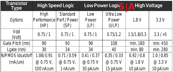
https://i.imgur.com/Y6qfWGl.png
Y6qfWGl.png


22FDX from May 2017:
https://i.imgur.com/CstBV6J.png
CstBV6J.png

In everything: Channel Length = Gate Length. As it is the Leff/Lgate or effective gate surface, etc.
 

Obvcop

Junior Member
Mar 7, 2017
11
12
36
Is there any actual real evidence from after the announcement (about canning new nodes) that glofo are still planning to go full steam ahead with 12fdx. Or has it been taken out the back yard and shot
 

Hitman928

Diamond Member
Apr 15, 2012
5,243
7,790
136
https://www.semiaccurate.com/wp-content/uploads/2012/12/Intel_22nm_table.png
Intel_22nm_table.png


22FFL numbers:
https://i.imgur.com/Y6qfWGl.png
Y6qfWGl.png


22FDX from May 2017:
https://i.imgur.com/CstBV6J.png
CstBV6J.png

In everything: Channel Length = Gate Length. As it is the Leff/Lgate or effective gate surface, etc.

Nope, your improperly cited "research" has failed you again, it is 26 nm.

https://en.wikichip.org/wiki/22_nm_lithography_process

https://www.researchgate.net/public...rst_commercial_tri-gate_high-k_metal-gate_CPU

Not sure why we are even discussing it though, the actual gate length has become less and less important with smaller nodes and the move to finfets.
 

NostaSeronx

Diamond Member
Sep 18, 2011
3,686
1,221
136
Is there any actual real evidence from after the announcement (about canning new nodes) that glofo are still planning to go full steam ahead with 12fdx. Or has it been taken out the back yard and shot
The only roadmap affected is the FinFET roadmap from: GlobalFoundries Press Release, Aug 27th 2018.
"GF is realigning its leading-edge FinFET roadmap to serve the next wave of clients that will adopt the technology in the coming years. The company will shift development resources to make its 14/12nm FinFET platform more relevant to these clients, delivering a range of innovative IP and features including RF, embedded memory, low power and more. To support this transition, GF is putting its 7nm FinFET program on hold indefinitely and restructuring its research and development teams to support its enhanced portfolio initiatives. This will require a workforce reduction, however a significant number of top technologists will be redeployed on 14/12nm FinFET derivatives and other differentiated offerings."

"GF is intensifying investment in areas where it has clear differentiation and adds true value for clients, with an emphasis on delivering feature-rich offerings across its portfolio. This includes continued focus on its FDXTM platform, leading RF offerings (including RF SOI and high-performance SiGe), analog/mixed signal, and other technologies designed for a growing number of applications that require low power, real-time connectivity, and on-board intelligence."

From the Report to EU Parliament, mid-2017:
"The results for this project are a technical success for supporting Soitec FDSOI business. In this project the SOI substrate technology blocks for 22FDX technology and 22FD+ were developed."
"A number of activities (outside the project) will transfer the pilot line to full size production facility: with 1st industrialization phase started in July 2017 in Soitec to catch 22FDX ramp. Due to the successes in this project significant investment was done in 2017 in the 300mm Bernin FDSOI fabrication line. This first investment phase is will be followed in 2018 with a second phase."

22FD+ became 22FDX+ as in this image: https://i.imgur.com/KOYu5AD.png
and I have previously talked about the Bernin II phases before in #283.

For 12FDX it was a spiral...
2016-
"Customer product tape-outs are expected to begin in the first half of 2019."
2017-
"The foundry is scheduled to move the 12FDX to risk production in the second half of 2018 followed by volume production in first-half 2019."
Which is verified in September 2017: https://forums.anandtech.com/thread...nce-applications.2519335/page-4#post-39089092
0.5PDK is risk production for GlobalFoundries.
1Q 2018: "We expect to be taking risk production on the parts early next year (2019), so we are pretty far along with the technology." - https://www.anandtech.com/show/1243...ew-with-dr-gary-patton-cto-of-globalfoundries
2Q 2018: "We expect tape outs on 12FDX in 2020 with deliveries in 2021." - http://www.eenewsanalog.com/news/globalfoundries-add-another-nvm-fdsoi/page/0/1
2H2018 - NostaQuess:
12FDX is being pushed further along to support 22FDX+. Which hopefully it will get inserted into the roadmap eventually.

22FDX (Power-optimized)
22FDX+ (Performance-optimized)
12FDX (Perf or Power-optimized separated in PDK extensions, not in node).

Also, Europe and China are throwing billions at GlobalFoundries. United States is giving zip, Saxony is thousands-millions, not even close to billions. Dresden/Chengdu are both declared foundries for FDSOI. So, Malta barely makes revenue targets and is a constant loss. Malta is a declared FinFET foundry, even though they do lab-work for 22FDX/22FDX+/12FDX. So, if FDSOI comes out specifically a net profit transistor type. Then, all the expenditures will revolve around the leading edge in FDSOI.

The only people who can steal customers from GlobalFoundries are: HLMC, Samsung, STMicroelectronics.
Samsung with two low-capacity FDSOI fabs => S1(Korea) & S2(America)
HLMC with one low-capacity FDSOI fab => H6(China)
STMicroelectronics with one low-capacity FDSOI fab but are now licensing from GlobalFoundries => France and Italy fabs are not competing.
GlobalFoundries will have two fabs: Fab 11(China-MegaFab) and Fab 1(Europe-GigaFab).

While, for FinFETs it will always be go TSMC. TSMC will probably provide better differentiated options for 16FF/12FF/10FF over GloFo's 14FF/12FF.

Hypothetically: If Apple lets say created an B-series on FDSOI, which is would be a budget form of the A-series. Only GlobalFoundries would be able to satisfy their order capacity of FDSOI.
 
Last edited:

DrMrLordX

Lifer
Apr 27, 2000
21,617
10,826
136

About that . . .


I know, right?

Not sure why we are even discussing it though, the actual gate length has become less and less important with smaller nodes and the move to finfets.

It's just Nosta being Nosta. If you're gonna be wrong about the future, you may as well be wrong about the past, too.

Is there any actual real evidence from after the announcement (about canning new nodes) that glofo are still planning to go full steam ahead with 12fdx. Or has it been taken out the back yard and shot

No real evidence of either outcome. The only thing that's for sure is that their 7nm FinFET node(s) is/are off the table for the foreseeable future. They came out and said, "We want to sell as many wafers as we can from fabs tooled for our existing nodes" more-or-less. Logic would indicate that the rate of invesetment in any future node would be reduced (if not zeroed out completely). GF isn't sharing their internal roadmaps with us, though (except NostaSeronX, teehee).
 

NostaSeronx

Diamond Member
Sep 18, 2011
3,686
1,221
136
https://www.digitimes.com/news/a20181026PR200.html
- Globalfoundries, Chengdu government realign JV strategy
Globalfoundries and the Chengdu municipality have signed an amendment to their investment and cooperation agreement. Based on market condition changes, Globalfoundries' renewed focus on differentiated offerings and discussions with potential clients, the two firms have decided to bypass the original phase one investment in mainstream process technology (180/130nm). It is also agreed that the project's timeline will be adapted to better align capacity to meet demand from China for differentiated offerings including Globalfoundries' 22FDX technology.
Phase one is bypassed and 22FDX is being accelerated and expanded(180/130 -> 22FDX) for Fab 11.
---
Within twelve months from now UMC will be taken private by GlobalFoundries/Mubadala w/ Chinese support.

---
- Possibility to extend to 7nm with performance booster already identified. Proof of concept demonstrated on silicon. /CEALeti
GlobalFoundries has licensed 2nd generation 7FD for 7FDX. Which is with the above performance booster.

On another note:
GlobalFoundries has rephrased its 7nm policy. It has cancelled 7nm FinFETs, but it will be coming out with 7nm Nanosheets. Post-7nm is still in discussion.

12FDX => 2020
New 7LP => 2021 (3 year delay as old 7LP went risk in Q1 2018... with new 7LP going risk in Q2 2021)
The delay is fiscal(wafers sold and demand) and cobalt(price skyrocket and CNTs are better).
 
Last edited:

Ajay

Lifer
Jan 8, 2001
15,429
7,847
136
On another note:
GlobalFoundries has rephrased its 7nm policy. It has cancelled 7nm FinFETs, but it will be coming out with 7nm Nanosheets. Post-7nm is still in discussion.
Do you have a link on that. This is a huge deal if true, even if the timeline is pushed out.