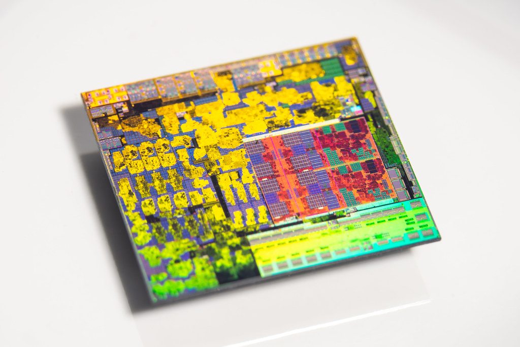
Question AMD Rembrandt/Zen 3+ APU Speculation and Discussion

Page 2 - Seeking answers? Join the AnandTech community: where nearly half-a-million members share solutions and discuss the latest tech.

izaic3

Member
Nov 19, 2019
61
96
61
Alright, so we've had some leaks so far. I don't know if any of it's been confirmed yet, as it's pretty early, but here is what I've surmised so far (massive grain of salt of course):

If if turns out to have RDNA 2 and 12 CU, I could see iGPU performance potentially almost doubling over Cezanne.

If I've made any mistakes or gotten anything wrong, please let me know. I'd also love to hear more knowledgeable people weigh in on their expectations.
 
Last edited:

andermans

Member
Sep 11, 2020
151
153
76
Pollock are the ULV chips, basically a 5W 14nm Raven2 that they are trying to cram into ultra-portable, tablets, chromebooks, etc. Something that is doomed to fail and it is going to cause more damage than good, it seems that they will never learn.

Dali is the replacement of Raven2, it is based on 12nm, and has 4 cores, 4 threads and Vega 3. Used on the 3050GE (2C/4T) and 3150G(4C/4T). They are OEM only just like Renoir.

I think Dali is raven2, instead of being a successor?

I believe a lot of the low end is likely to be served reasonably well by lucienne/barcelo/(rembrandt follower) and only for really low end ( like <300$ laptops) you really need one of the smaller chips. I wonder if this is because due to AMDs small market share in laptops it may be cheaper for them to save on development costs than save on production costs? Or is the scale already big enough that this doesn't matter?
 

LightningZ71

Golden Member
Mar 10, 2017
1,627
1,898
136
It still feels like AMD needs a "half Lucienne" product with a single 4-core CCX and Vega 4CU. It should be roughly 60% the size of the Lucienne die and would give many more chips per wafer. Yes, it will be more expensive to make than Dali or Pollock, but, it will be much more performant from both a throughput and a power draw perspective.

As for Pollock, it will still be a massive upgrade from the zombie construction core products that AMD has been offering in that market for much of the last half decade.
 

Shivansps

Diamond Member
Sep 11, 2013
3,835
1,514
136
I think Dali is raven2, instead of being a successor?

Yeah i dont really know for sure at this point anymore, information is all messed up, i know is that there are both Dual and Quad core Athlons.

One is a dual core Zen APU with Vega 3 on 14nm ( Athlon 3000G, Athlon 3050U, Athlon 3150U, Athlon 3050GE ), this is Raven2.

The other is a quad core Zen+ APU with Vega 3 on 12nm ( Athlon 3150G, Athlon 3150GE ).

There is a posibility of the 3150G/GE being a cut down Picasso, if this is the case ill never know why they decided to cut the IGP that much.
 

andermans

Member
Sep 11, 2020
151
153
76
Yeah i dont really know for sure at this point anymore, information is all messed up, i know is that there are both Dual and Quad core Athlons.

One is a dual core Zen APU with Vega 3 on 14nm ( Athlon 3000G, Athlon 3050U, Athlon 3150U, Athlon 3050GE ), this is Raven2.

The other is a quad core Zen+ APU with Vega 3 on 12nm ( Athlon 3150G, Athlon 3150GE ).

There is a posibility of the 3150G/GE being a cut down Picasso, if this is the case ill never know why they decided to cut the IGP that much.

I think it is just cut down Picasso. Would really surprise me if there is is an extra chip. AFAIU Raven2 is basically 2 core Zen+, so both Dali and Pollock.
 

LightningZ71

Golden Member
Mar 10, 2017
1,627
1,898
136
Is it an actual cut-down Picasso with fewer actual CUs on die, or is it actually just a die recovery project for Picasso that recovers die with failed CUs? The die space saved by shaving off the 8 remaining CUs (11 total down to 3) is not massive. And why go that route? Their biggest competition in the bottom end of the windows notebook market is the i3-1005g1 and i3-1115G4. Both are dual core lake based processors with a modest, but still usable iGPU. It seems to me that a good counter to those products would have been a 14nm 2 x Zen2 core CCX with 4MB L3 and 5 vega CUs. It would still be smaller than Picasso, but outperform everything below the 3200g/3400g/3500u/3700u.
 

LightningZ71

Golden Member
Mar 10, 2017
1,627
1,898
136
I apologize if I wasn't clear. I was referring to this section...

-----------------------------------------------
The other is a quad core Zen+ APU with Vega 3 on 12nm ( Athlon 3150G, Athlon 3150GE ).

There is a posibility of the 3150G/GE being a cut down Picasso, if this is the case ill never know why they decided to cut the IGP that much.
------------------------------------------------

Is the Quad core Athlon actually a cut down Picasso, or is it it's own somewhat shrunken die? It's hard to imagine a die so badly crippled in the smaller iGPU area that it has to be cut down to 3 CU from a total of 11 present that still allows four functional cores.
 

jpiniero

Lifer
Oct 1, 2010
14,510
5,159
136
Is the Quad core Athlon actually a cut down Picasso, or is it it's own somewhat shrunken die? It's hard to imagine a die so badly crippled in the smaller iGPU area that it has to be cut down to 3 CU from a total of 11 present that still allows four functional cores.

It happens enough that they made an SKU out of it. You're scraping the bottom of the barrel, that's what Athlon is for.
 

IntelUser2000

Elite Member
Oct 14, 2003
8,686
3,785
136
Is the Quad core Athlon actually a cut down Picasso, or is it it's own somewhat shrunken die? It's hard to imagine a die so badly crippled in the smaller iGPU area that it has to be cut down to 3 CU from a total of 11 present that still allows four functional cores.

Sometimes, the manufacturer will take a 6CU die and disable 3 of them to sell it as a 3CU part as relying only on a defective part will not satisfy the massive volume requirements of a low end SKU.

This is assuming AMD really only uses 1 die.

The silicon costs are a small portion of the final price. Probably $15 die and $5 packaging? This is why they have some flexibility playing the market. The rest are to make up for revenue/profit requirements and paying for labor, fabrication facilities, research, etc.
 

Mopetar

Diamond Member
Jan 31, 2011
7,797
5,899
136
AMD only uses a single die for their APUs although there're some cases like now where both Cezanne and Lucienne exist simultaneously while being different designs, but within both there's 4/6/8-core parts.
 

Shivansps

Diamond Member
Sep 11, 2013
3,835
1,514
136
Im wondering how they will do the Raphael IGP... either a small IGP on I/O die, or a GPU chiplet... specially considering that GPU chiplets will happen at some point.
 

TESKATLIPOKA

Platinum Member
May 1, 2020
2,329
2,811
106
There was a discussion about how powerful is RDNA2 IGP compared to RX560 and RX570 so let's continue here.
Specs:
RX 560 16CU(1024:64:16, 112GB/s) base frequency: 1175(turbo 1275)Mhz -> 2.41(2.61)TFlops
RX 570 32CU(2048:128:32, 224GB/s) base frequency: 1168(turbo 1244)Mhz -> 4.78(5.1)TFlops
My speculation for a mobile variant specs:
RDNA2 IGP 12CU(768:48:16, ?GB/s) base frequency: 1600(turbo 2000)Mhz -> 2.46(3.1)TFlops -> * 1.35 = 3.32(4.19)TFlops

Conclusion:
This IGP shouldn't have any problem outperforming RX560 by a large margin unless bandwidth will turn out as a massive bottleneck, but then why put 12CU in this APU, right?
On the other hand the situation for RX570 is much better. At worst It's only 22% or at best 44% faster depending on how high can Rembrandt's IGP keep Its clocks.
Let's not forget I am comparing desktop cards with 60-80W and 150W TBP(whole card) against a mobile APU's IGP limited to 45W(CPU+IGP) TDP.
Desktop Rembrandt version could very well be clocked to 2.5GHz or more and still be within 95W TDP, that would give It at least 3.88TFlops and with 35% better performance per TFlop, It would be equivalent to 5.24TFlops, and now It's comparable to RX 570.
Now the question is how much BW is needed. For the mobile 2GHz variant I would recommend at least 6.4GHz 128bit DDR5(102.4 GB/s), for desktop version even more.

P.S. This was only an example, doesn't represent the actual performance or specs.
 
Last edited:
  • Like
Reactions: Tlh97

IntelUser2000

Elite Member
Oct 14, 2003
8,686
3,785
136
I'm not as optimistic at the iGPU performing that well. Actually they perform somewhat under spec. It's because they have to share both power and memory.

The memory sharing part reduces performance by 10-20%, because you can't be perfect and there will always be contention which reduces performance in terms of both latency and bandwidth, even if the CPU doesn't require a lot.

While AMD gained great deal of efficiency and performance with RDNA2, the die size grew 100% to do so. If you compare Vega to RDNA, the performance is similar, but RDNA requires 250mm2 versus Vega's 330mm2. But they also cut resources by 33%.

Vega CU = RDNA 0.67 CU, with smaller die.
RDNA CU = Vega CU x 1.3x performance.
RDNA2 1.5x CU = Same power efficiency as RDNA CU, but potentially 2x the die size

The desktop Polaris/Vega parts also ran way beyond a reasonable level to achieve their performance. There was a whole discussion about this and were pleasantly surprised that Vega 11 was efficient, since it didn't have to reach that high.

Polaris/Vega owners also know they can undervolt/underclock them quite a bit.
 

Shivansps

Diamond Member
Sep 11, 2013
3,835
1,514
136
As things a are right now, a 3400G with DDR4-3200 is around -15% the performance of a 4GB RX550 with 8CU Polaris and 112GB/s 128bit GDDR5. I think it is safe to say that a 2.5Ghz Vega 8 on Cezanne with DDR4-3600 will already match the RX550 and outperform it in a few cases.
Now, the RX560 is not that far away from that as you may think, in fact if Cezanne had 11CU it would be very very close or it would already match it. Not sure what the bottleneck on Polaris is but going from 8CU to 16CU does yields around 30% gains.


So, things have to go VERY wrong for 12CU RDNA2 and DDR5 not to outperform the RX560 by a huge margin. And something is very wrong with Polaris that a Vega 8 at 2.3Ghz and shared DDR4-4000 can get that close to a 16CU GPU with 128bit GDDR5.

The problem i see is that the RX570 is around 80% faster than the RX560, so it may fall a little short, so non-super GTX1650 is more likely for the 12CU IGP and RX570 by overcloking.
 
Last edited:
  • Like
Reactions: Tlh97

TESKATLIPOKA

Platinum Member
May 1, 2020
2,329
2,811
106
I'm not as optimistic at the iGPU performing that well. Actually they perform somewhat under spec. It's because they have to share both power and memory.

The memory sharing part reduces performance by 10-20%, because you can't be perfect and there will always be contention which reduces performance in terms of both latency and bandwidth, even if the CPU doesn't require a lot.
As I mentioned It was just an example and the performance can differ compared to this.

While AMD gained great deal of efficiency and performance with RDNA2, the die size grew 100% to do so. If you compare Vega to RDNA, the performance is similar, but RDNA requires 250mm2 versus Vega's 330mm2. But they also cut resources by 33%.

Vega CU = RDNA 0.67 CU, with smaller die.
RDNA CU = Vega CU x 1.3x performance.
RDNA2 1.5x CU = Same power efficiency as RDNA CU, but potentially 2x the die size
You have a mistake in Vega CU = RDNA 0.67 CU.... It should be 0.77 instead of 0.67, If you were talking about performance.

Navi 10 vs Vega 20
Specs: 40CU(2560:160:64), 256bit GDDR6 vs 60CU(3840:240:64), 4096bit HBM2
Size: 251 mm2 vs 331 mm2 (+32%)
TBP: 225W vs 300W (+33%)
The same performance with a smaller die size and power draw without using expensive HBM2, which BTW saves some additional die space and power compared to GDDR6.

Navi 10 vs Navi 22
Specs: 40CU(2560:160:64), 256bit GDDR6 vs 40CU(2560:160:64), 192bit GDDR6, 96MB IC
Size: 251mm2 vs 335 mm2(+33.5%)
TBP: 225W vs 230W (+2%)
Performance: 26-32% higher for Navi22 depending on resolution(Link)
So Navi 22 is more power efficient than Navi10 and the difference of 84mm2 in die size is mostly thanks to 96MB Infinity cache. RDNA2 CU should be bigger, but I think only by 10-15% at most and let's not forget about the added RT functionality.

Navi 22 vs Vega 20
Specs: 40CU(2560:160:64), 192bit GDDR6, 96MB IC vs 60CU(3840:240:64), 4096bit HBM2
Size: 335 mm2 vs 331 mm2 (-1%)
TBP: 230W vs 300W (+30.4%)
Performance: 26-29% higher for Navi22 depending on resolution (link above) and efficiency by 64-68% depending on resolution.

I don't know why you think die size grew by 100% when It's actually comparable(Navi22 vs Vega20). Even If you were talking only about CU size, that's also not true based on specs.

The desktop Polaris/Vega parts also ran way beyond a reasonable level to achieve their performance. There was a whole discussion about this and were pleasantly surprised that Vega 11 was efficient, since it didn't have to reach that high.
So was RX 5700XT and now RX 6700XT.

Polaris/Vega owners also know they can undervolt/underclock them quite a bit.
You can do the same with RDNA2 with pretty good results.
 
Last edited:
  • Like
Reactions: Tlh97

LightningZ71

Golden Member
Mar 10, 2017
1,627
1,898
136
I doubt that we're ever going to see more than 102ish GB/sec in a DDR5 APU simply because thatythe (current) JEDEC limit of the spec for 128bits. Mobile will be lower for a long time due to power and thermals. That doesn't have to be the effective limit for performance. While an APU doesn't have to have a huge Infinity Cache, just upping the L3 cache for the APU to the desktop level of 32MB and intelligently partitioning it to reserve 24MB for the iGPU when it detects heavy use will go a long way to making up for the lower memory bandwidth out to the modules.

The other thing that people are seeing when looking at the memory bandwidth contention on the existing APUs is the small L3 cache that most have had till this most recent generation. Raven Ridge had 1MB per core. Renoir had 1+1.5 MB per core. Cezanne has 2-3MB per core. Across the aisle, Intel outfits Tiger Lake U with up to 3MB per core. People wonder how Intel is getting so much performance from their iGPU, and aside from good design, having a fair bit less contention for memory bandwidth due to having a larger L3 can't be hurting anything. Their APUs don't need to have an "infinity cache" per se, just having a large L3 alone can help things, even if it isn't doing anything special.
 

Mopetar

Diamond Member
Jan 31, 2011
7,797
5,899
136
Conclusion:
This IGP shouldn't have any problem outperforming RX560 by a large margin unless bandwidth will turn out as a massive bottleneck, but then why put 12CU in this APU, right?

I suspect that once we see RDNA2 incorporated into APUs we also see something similar to infinity cache which helps alleviate a lot of bandwidth issues. There's already 16 MB of L3 cache, so it doesn't seem out of the realm of possibility for AMD to double it and make it a unified cache accessible to both the CPU and GPU.

In some ways the inclusion of infinity cache in RDNA2 may have been influenced by a desire to solve the bandwidth limitations that integrated graphics face, because AMD could have just as easily gone with a wider bus, likely to similar effect, with their Navi cards. From AMD's slides, even a 32 MB infinity cache produced a hit rate above 50% for 1080p gaming.

Even if someone isn't going to do much or any gaming on their APU, I've no doubt that there are a lot of other applications that would benefit from a CPU with an even larger cache, so it's not even all that wasteful.
 
  • Like
Reactions: Tlh97

andermans

Member
Sep 11, 2020
151
153
76
I suspect that once we see RDNA2 incorporated into APUs we also see something similar to infinity cache which helps alleviate a lot of bandwidth issues. There's already 16 MB of L3 cache, so it doesn't seem out of the realm of possibility for AMD to double it and make it a unified cache accessible to both the CPU and GPU.

In some ways the inclusion of infinity cache in RDNA2 may have been influenced by a desire to solve the bandwidth limitations that integrated graphics face, because AMD could have just as easily gone with a wider bus, likely to similar effect, with their Navi cards. From AMD's slides, even a 32 MB infinity cache produced a hit rate above 50% for 1080p gaming.

Even if someone isn't going to do much or any gaming on their APU, I've no doubt that there are a lot of other applications that would benefit from a CPU with an even larger cache, so it's not even all that wasteful.

Linux drivers indicate VanGogh doesn't have infinity cache ( ). Of course people may be misinterpreting that and we could have some not quite infinity cache or it might be added in Rembrandt but at this point I'm mostly sceptical about a bunch of cache getting added.
 

Shivansps

Diamond Member
Sep 11, 2013
3,835
1,514
136
I dont think they are going for IC on the 1st iteration of RDNA APUs. BUT, if Raphael ends up having a chiplet iGPU, those chiplets may contain some sort of IC.
 

IntelUser2000

Elite Member
Oct 14, 2003
8,686
3,785
136
So was RX 5700XT and now RX 6700XT.


You can do the same with RDNA2 with pretty good results.

Yes, but the RX 5700/6xxx series are actually competitive, so they didn't need to push it as far. Vega wasn't, so to get closer to competition in terms of performance they had to jack up clocks.

I was actually comparing it to the 6800/6800XT.

My point is they still had to cut down the CUs to get that area. Vega 20 is at 330mm2 but grow to 520mm2 with Navi 21. 1.5x SP of Vega 20 will push it to the 600mm2 range.

Going from Vega 8 to Navi 12 will double the iGPU size as well.