AMD GDC2016 Thread

Page 11 - Seeking answers? Join the AnandTech community: where nearly half-a-million members share solutions and discuss the latest tech.

pandemonium

Golden Member
Mar 17, 2011
1,777
76
91
What the average length a normal person games daily? Then what is the average for vr gamers? If this can do 2 hours untethered, that might be enough.


Per week.

5-6.5hrs.

That statistic is for amount of time played with others online, not amount of time played in general. This is a more accurate representation of time spent gaming in general for the same year (2014).
 
Feb 19, 2009
10,457
10
76
Is it possible a 232mm2 14 FF Polaris being faster than Fury X? o_O

That would be approaching the "too good to be true" realm.
 

crisium

Platinum Member
Aug 19, 2001
2,643
615
136
It would be a failure if one Polaris card did not beat the Fury X, I don't care if Vega is the real deal. Can you imagine the 7970 or 680 losing to the 6970 or 580? It didn't matter that 290X and 780 Ti were yet to come, a new node and new architecture combined should mean better performance. I know that the 7970 was only slightly smaller than the 6970 and that Polaris vs Fiji die size difference is far, far larger, but it's the principle of the thing.
 

Glo.

Diamond Member
Apr 25, 2015
5,657
4,409
136
I have the same problem in believing this, even if reality looks that way.

4096 GCN4 core GPU with HBM1 without any of the bottlenecks of Fury X?
 

Head1985

Golden Member
Jul 8, 2014
1,863
685
136
Is it possible a 232mm2 14 FF Polaris being faster than Fury X? o_O
Nope unless AMD pulls their own 8800GTX.
We know FIJI design sucks and its bottleneck.
Now FURY X is only 14-20% faster than 390x in 1080p.SO if they increase SP performance by 20-30% and it will have 2800-3000SP it will be faster than FURY X.

Yeah it is possible if they increase SP performance.FIJI is just awful bad design.
 
Last edited:

Glo.

Diamond Member
Apr 25, 2015
5,657
4,409
136
2.5 times better performance per watt?

Fury X has 8.6 TFLOPs of compute power. Dividing it by 275W gives us around 31 GLOPs/W.
Times 2.5 we are around 9.7 TFLOPs of compute power at 125W.
5120 GCN cores at 950 MHz are giving similar amount of power.

It does not mean anything. It is just me doing math :p. Do not extrapolate anything from this :D. It is just a perspective of what we are having here.
 

raghu78

Diamond Member
Aug 23, 2012
4,093
1,475
136
Is it possible a 232mm2 14 FF Polaris being faster than Fury X? o_O

That would be approaching the "too good to be true" realm.

Polaris is the first major architectural improvement to GCN in 4 years. I expect it to be a major leap in perf and efficiency . The last time AMD had a process node change + major architectural improvement, the HD 7870 beat the HD 6970 (prev gen flagship). I think such a situation is very much possible with the high end Polaris 10 SKU beating the Fury X. btw if you look at the 2.5x perf/watt increase with Polaris , Fiji perf at 275w should now be acheivable at 275/2.5 = 110w. There is room for slightly higher perfomance with a slightly higher TDP.
 

maddie

Diamond Member
Jul 18, 2010
4,722
4,625
136
Remember when we heard 2X perf/watt increase. Now one seems to be hearing 2.5X perf/watt more frequently.
AMD also claimed that 70% of this would be 14nm effect and 30% would be architectural improvements.

Putting these together and assuming that the 14nm finfet benefit is a fixed quantity, we end up with the architecture gains as much larger than first estimated.

Remember that in the Polaris 11 demo it was mentioned that a lot of power optimizations are still to come. With these in place the option to clock higher becomes available.
 

MrTeal

Diamond Member
Dec 7, 2003
3,554
1,658
136
I have the same problem in believing this, even if reality looks that way.

4096 GCN4 core GPU with HBM1 without any of the bottlenecks of Fury X?

That seems really unlikely. First they'd really need to get 8Hi working in order to get a modern amount of memory on it. 4GB wouldn't cut it in that performance bracket anymore. If they reduced the bottlenecks in Fiji's design that would if anything add more transistors. Architectural improvements generally also cost transistors. Given Fiji's already at 8.9B, a 4096 shader Polaris 10 could be 10B, or even more if they need to go with 8 stacks of HBM1. That's around 2.9x the transistor density of Fiji, which given GloFo's guidance to expect 2x that seems improbably.

Now, a Hawaii sized GPU (shader wise) with architectural improvements and maybe some clock speed improvements bridging the 25% percent gap we see to Fury X? That I could see, and ~3k shaders seems perfectly reasonable to fit on a 232mm² die.

OFC, always with the assumption that the die is 232mm².
 

ShintaiDK

Lifer
Apr 22, 2012
20,378
145
106
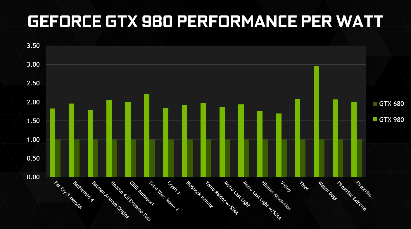
Be careful with the 2½x performance/watt. It may only be for a specific SKU or a specific game. And I am quite sure there is an "up to" note hidden somewhere. Polaris 10 and 11 should also both be GDDR5(x).

Remember this?
nvidia-maxwell-architecture-performance-per-watt.png


Up to 3x performance/watt ;)
 

raghu78

Diamond Member
Aug 23, 2012
4,093
1,475
136
Be careful with the 2½x performance/watt. It may only be for a specific SKU or a specific game. And I am quite sure there is an "up to" note hidden somewhere. Polaris 10 and 11 should also both be GDDR5(x).

Remember this?
nvidia-maxwell-architecture-performance-per-watt.png


Up to 3x performance/watt ;)

Very simple. AMD gave a 70/30 split for power efficiency improvements from process node and architecture.

http://www.pcper.com/reviews/Graphi...hnologies-Group-Previews-Polaris-Architecture

"How is Polaris able to achieve these types of improvements? It comes from a combination of architectural changes and process technology changes. Even RTG staff were willing to admit that the move to 14nm FinFET process tech was the majority factor for the improvement we are seeing here, something on the order of a 70/30 split. That doesn’t minimize the effort AMD’s engineers are going through to improve on GCN at all, just that we can finally expect to see improvements across the board as we finally move past the 28nm node."

70/100 * 2.5 = 2.05
30/100 * 2.5 = 0.45

We know that 14nm FINFET provides a 2x power efficiency improvement over 28nm. This agrees with the above calculation. So out of the 150% perf/watt gain, 105% is from process and the rest 45% is from architecture. We will know when the reviews are out whether the perf/watt gain statement is accurate or not. But I think its possible.
 

Stormflux

Member
Jul 21, 2010
140
26
91
WTF, is Nvidia opening Gameworks? Maybe they found out AMD will add extreme tesellation in Polaris and there is no point anymore ?:p
Just Kidding, I guess they just have enough of internet wars. Thank god...
http://www.pcper.com/reviews/Graphics-Cards/Details-about-NVIDIAs-GameWorks-31-Update
nvidia-2016-gdc-open-list.png


Coming soon = after extreme tesellators in AMD are confirmed. Stupid joke ,sry :<

This is great and all but it all depends on the licensing going forward. AMD GPUOPen uses an MIT License. Which is more advantageous to the cause than GPL. Do we know what license scheme nVidia is using for the GitHub accessible code?
 

ElFenix

Elite Member
Super Moderator
Mar 20, 2000
102,414
8,356
126
The interesting cost scenario for HBM2 is on CPU/APUs. On GPUs you need its RAM pool one way or the other, its a matter of what it costs and how fast it is. With CPUs and APUs you dont include the RAM, thats an assumed extra cost. But if you interposed HBM along with an APU/CPU you increase cost that goes to you while eliminating the RAM cost on the end user's side. This math could work out favorably because the end user sees marked-up, full distribution to consumer prices for RAM where the HBM would be available to AMD @ volume prices straight from the manufacturer. So while the costs for RAM are lower in reality, the marked up end user price may not be so far off from the real cost of HBM. I dont have the numbers so I could be off, but its a more interesting equation than GDDR5 vs HBM straight across

you also vastly simplify motherboard design. i don't know if i see HBM as a solution for desktop parts, but it'd be very useful in notebook parts - just even further on down the system-on-a-chip path.
 

MrTeal

Diamond Member
Dec 7, 2003
3,554
1,658
136
The interesting cost scenario for HBM2 is on CPU/APUs. On GPUs you need its RAM pool one way or the other, its a matter of what it costs and how fast it is. With CPUs and APUs you dont include the RAM, thats an assumed extra cost. But if you interposed HBM along with an APU/CPU you increase cost that goes to you while eliminating the RAM cost on the end user's side. This math could work out favorably because the end user sees marked-up, full distribution to consumer prices for RAM where the HBM would be available to AMD @ volume prices straight from the manufacturer. So while the costs for RAM are lower in reality, the marked up end user price may not be so far off from the real cost of HBM. I dont have the numbers so I could be off, but its a more interesting equation than GDDR5 vs HBM straight across

you also vastly simplify motherboard design. i don't know if i see HBM as a solution for desktop parts, but it'd be very useful in notebook parts - just even further on down the system-on-a-chip path.

The mobile/AOI market is a natural choice as those are often designed with limited upgradeability in mind. It would be an interesting cost analysis though, even in desktops. Yes, APU + HBM + interposer costs more than a straight CPU + DDR4 chips, but you eliminate a bunch of other parts. As you say, you simplify the MB, potentially allowing fewer layers and reducing the size of it (much easier to build mATX or mITX, for instance). You also eliminate at the least two DIMM slots, as well as the DIMM PCB, assembly, packaging and shipping costs. I'm not sure how much more expensive the HBM APU would be even vs CPU + RAM before markup.

A minor downside for people is lack of upgradeability, but I would question how many people buying small desktops with APUs actually perform RAM upgrades.
 

Bacon1

Diamond Member
Feb 14, 2016
3,430
1,018
91
This is great and all but it all depends on the licensing going forward. AMD GPUOPen uses an MIT License. Which is more advantageous to the cause than GPL. Do we know what license scheme nVidia is using for the GitHub accessible code?

Copyright 2014-2016 NVIDIA Corporation

BY DOWNLOADING THE SOFTWARE AND OTHER AVAILABLE MATERIALS, YOU ("DEVELOPER") AGREE TO BE BOUND BY THE FOLLOWING TERMS AND CONDITIONS

The materials available for download to Developers may include software in both sample source ("Source Code") and object code ("Object Code") versions, documentation ("Documentation"), certain art work ("Art Assets") and other materials (collectively, these materials referred to herein as "Materials"). Except as expressly indicated herein, all terms and conditions of this Agreement apply to all of the Materials.

Except as expressly set forth herein, NVIDIA owns all of the Materials and makes them available to Developer only under the terms and conditions set forth in this Agreement.

License: Subject to the terms of this Agreement, NVIDIA hereby grants to Developer a royalty-free, non-exclusive license to possess and to use the Materials. The following terms apply to the specified type of Material:

Source Code: Developer shall have the right to modify and create derivative works with the Source Code. Developer shall own any derivative works ("Derivatives") it creates to the Source Code, provided that Developer uses the Materials in accordance with the terms of this Agreement. Developer may distribute the Derivatives, provided that all NVIDIA copyright notices and trademarks are used properly and the Derivatives include the following statement: "This software contains source code provided by NVIDIA Corporation."

Object Code: Developer agrees not to disassemble, decompile or reverse engineer the Object Code versions of any of the Materials. Developer acknowledges that certain of the Materials provided in Object Code version may contain third party components that may be subject to restrictions, and expressly agrees not to attempt to modify or distribute such Materials without first receiving consent from NVIDIA.

Art Assets: Developer shall have the right to modify and create Derivatives of the Art Assets, but may not distribute any of the Art Assets or Derivatives created therefrom without NVIDIA&#65533;s prior written consent.

Government End Users: If you are acquiring the Software on behalf of any unit or agency of the United States Government, the following provisions apply. The Government agrees the Software and documentation were developed at private expense and are provided with &#65533;RESTRICTED RIGHTS&#65533;. Use, duplication, or disclosure by the Government is subject to restrictions as set forth in DFARS 227.7202-1(a) and 227.7202-3(a) (1995), DFARS 252.227-7013(c)(1)(ii) (Oct 1988), FAR 12.212(a)(1995), FAR 52.227-19, (June 1987) or FAR 52.227-14(ALT III) (June 1987),as amended from time to time. In the event that this License, or any part thereof, is deemed inconsistent with the minimum rights identified in the Restricted Rights provisions, the minimum rights shall prevail.
No Other License. No rights or licenses are granted by NVIDIA under this License, expressly or by implication, with respect to any proprietary information or patent, copyright, trade secret or other intellectual property right owned or controlled by NVIDIA, except as expressly provided in this License.
Term: This License is effective until terminated. NVIDIA may terminate this Agreement (and with it, all of Developer&#65533;s right to the Materials) immediately upon written notice (which may include email) to Developer, with or without cause.

Support: NVIDIA has no obligation to support or to continue providing or updating any of the Materials.

No Warranty: THE SOFTWARE AND ANY OTHER MATERIALS PROVIDED BY NVIDIA TO DEVELOPER HEREUNDER ARE PROVIDED "AS IS." NVIDIA DISCLAIMS ALL WARRANTIES, EXPRESS, IMPLIED OR STATUTORY, INCLUDING, WITHOUT LIMITATION, THE IMPLIED WARRANTIES OF TITLE, MERCHANTABILITY, FITNESS FOR A PARTICULAR PURPOSE AND NONINFRINGEMENT.

LIMITATION OF LIABILITY: NVIDIA SHALL NOT BE LIABLE TO DEVELOPER, DEVELOPER&#65533;S CUSTOMERS, OR ANY OTHER PERSON OR ENTITY CLAIMING THROUGH OR UNDER DEVELOPER FOR ANY LOSS OF PROFITS, INCOME, SAVINGS, OR ANY OTHER CONSEQUENTIAL, INCIDENTAL, SPECIAL, PUNITIVE, DIRECT OR INDIRECT DAMAGES (WHETHER IN AN ACTION IN CONTRACT, TORT OR BASED ON A WARRANTY), EVEN IF NVIDIA HAS BEEN ADVISED OF THE POSSIBILITY OF SUCH DAMAGES. THESE LIMITATIONS SHALL APPLY NOTWITHSTANDING ANY FAILURE OF THE ESSENTIAL PURPOSE OF ANY LIMITED REMEDY. IN NO EVENT SHALL NVIDIA&#65533;S AGGREGATE LIABILITY TO DEVELOPER OR ANY OTHER PERSON OR ENTITY CLAIMING THROUGH OR UNDER DEVELOPER EXCEED THE AMOUNT OF MONEY ACTUALLY PAID BY DEVELOPER TO NVIDIA FOR THE SOFTWARE OR ANY OTHER MATERIALS.

https://github.com/NVIDIAGameWorks/FaceWorks/blob/master/license.txt