AMD Bristol/Stoney Ridge Thread

Page 64 - Seeking answers? Join the AnandTech community: where nearly half-a-million members share solutions and discuss the latest tech.

Abwx

Lifer
Apr 2, 2011
10,947
3,457
136
AMD used GF because they had by contract. Even then, the GF 28 nm node certainly wasn't bad and was just a little behind TSMC. That's a completely different situation.

Actually GF s 28nm was much better than TSMC s, to the point that AMD had to reclassify the TSMC manufactured 4C Jaguar as 25W TDP.
Once it was ported to GF s 28nm as Puma s cores it was within the 15W targeted at the first place.


Hitman928

Diamond Member
Apr 15, 2012
5,262
7,890
136
Actually GF s 28nm was much better than TSMC s, to the point that AMD had to reclassify the TSMC manufactured 4C Jaguar as 25W TDP.
Once it was ported to GF s 28nm as Puma s cores it was within the 15W targeted at the first place.


I was referring more to when the nodes were available for HVM. TSMC 28 was a couple of years ahead of GF from what I remember, but it's been close to decade now so my memory might be a little fuzzy on exact timeline.
 

NostaSeronx

Diamond Member
Sep 18, 2011
3,686
1,221
136
BTW, here are actual GF materials that I've still seen used today. Notice what they say 22FDX is optimized for / targets and what they don't mention.
The same thing can be said for 28nm btw. However, AMD still used it even after it came out.

22fdxbias1.png
22fdxbias2.png
22fdxbias3.jpeg

This however ignores 22FDX+(September 2020), which has an improved transistor w/ Tsi=5.xnm and buried oxide height of 15nm. With 22FDX+ and 12FDX sharing performance and power of transistor designs, hence not needing 12FDX for a shrink.

1. Cost is lower.
2. Performance is higher.
3. Power is lower.
4. Area is lower.

High performance is included into Ultra-low-power with 8T-DBB/8T-CNRX (Ultra-low-power) being faster than 12T-DDB (Ultra-High-Performance). UHP through 8T-CNRX/8T-DDB is preferred for Cortex A72/A73 HiPerf CPU designs.

104CPP-8T in turn is faster than 78CPP-10.5T through 84CPP-7.5T. UHP replaces SHP without needing a new process to do it, unlike 28SHP vs 28SLP.

Geode LX 130nm during 90nm K8 and 65nm K8.
Bobcat on TSMC's 40nm during TSMC's 28nm era.
Puma in Bhavani GF 28nm during GlobalFoundries' 20nm/14nm and TSMC's 20nm/16nm push. (2014 - Bhavani AM1 would have continued to be on 28nm throughput Nolan/Catamount 20nm and Nolan+/Margay 14nm)

Significant trailing gives 22FDX+ a non-rushed design that can push ULP to HPinLP.
2016-2018 => ULP CPU&GPU
2019-present => ULP SoC

14LPP/12LP+ 0.5V-op = 800 MHz Target, but bins are 400 MHz. Do to gate effects and delay variation.
22FDX 0.5V-op = 2 GHz target, but bins are 2 GHz. Less gate effects and reduced delay variation plus margin control with FBB, too much delay add Vbb.

2019 EDA-company#1/#2 tools support ABB in 2019.
2020 GlobalFoundries announces 22FDX+ and EDA-company#1/#2/#3 announce ML-Synthesis and ML-DFM.

22fdxmobility.jpeg
22fdxmobility2.jpeg

1.49 “Fusion Products” shall mean both (a) MPU Products that incorporate GPU Products and ...,.
1.58 “MPU Products” shall mean any of the following: (i) the x86, x86-64, and IA (Intel Architecture)-64 families of microprocessors, (ii) any existing or new microprocessors based on the x86, x86-64, and IA-64 family architecture, or any new instruction set for a processor described in clause (i) first introduced by AMD, (iii) any microprocessors based on new architecture or an architecture adopted in the future, or (iv) Fusion Products. As used in this definition, a microprocessor shall include a component that can execute computer programs and is the central processing unit controlling an electronic device.

Bobcat is a MPU/Fusion product. ULP CPU&GPU is a MPU/Fusion product.

14LPP goes on Performance-track because it doesn't scale well in extreme power settings. While 22FDX goes Power-track because it does scale well in extreme power settings.

Bobcat (CMP) -> Jaguar/Puma (CMP) -> Excavator (CMT) -> New ULP CPU architecture (CMT, but with ~90% perf at half-area, +1 GHz clock-rate)
VLIW4 -> GCN -> GCN3 -> New ULP graphics architecture (Small RDNA/CDNA -hybrid, small dispatches and high scalar FP64, packed FP32/FP16/INT16/INT8 rate)
 
Last edited:
  • Like
Reactions: Tlh97 and Zepp

Hitman928

Diamond Member
Apr 15, 2012
5,262
7,890
136
The same thing can be said for 28nm btw. However, AMD still used it even after it came out.

Again, AMD had to by contract. Additionally, GF 28nm was a solid node, it was just a little later than TSMC's node but it's not like today where there were far superior nodes available for AMD to develop on. The 28 nm nodes were actually very long lived and the world (outside of Intel) were stuck on them for quite a while because the non-Intel 20/22 nm nodes sucked and it took significant time for TSMC and GF to get Finfets up and running.


More images without context or sourcing. Do you know what type of FETs they are comparing? Even if they were making the proper comparison for high performance FETs (which I doubt, this is most likely promoting low freq, low power FETs which 22FDX does better at compared to high performance FETs), it still requires back body biasing to get to 14nm levels which took the ecosystem years to get right and still to this day I don't believe has actually been used on any large SOC designs because of the added complexity and risk and availability of Finfet nodes.

This however ignores 22FDX+(September 2020), which has an improved transistor w/ Tsi=5.xnm and buried oxide height of 15nm. With 22FDX+ and 12FDX sharing performance and power of transistor designs, hence not needing 12FDX for a shrink.

1. Cost is lower.
2. Performance is higher.
3. Power is lower.
4. Area is lower.

22FDX was announced in Sep. 2020 but wasn't available to use until some time in 2021 and even then was only made available for the RF flavor/library. You have to wait if you are not using the RF version (which you wouldn't be for these types of designs). They will also still need 12FDX at some point, 22FDX+ is a nice improvement, but it's not a replacement for 12FDX, whenever they can actually get it available. So maybe in 2022 you could come out with a high performance design that rivals what you could have made on 14 LPP, what, 5 years earlier(?), and will still be blown away by any modern design put out by your competitors on more advanced nodes. Not exactly a winning strategy. Let me know when we start to see anyone doing high performance designs jumping on 22FDX+, I have a feeling I will be waiting a very long time.

High. . .

More just random. . . something?

View attachment 54462
View attachment 54463

1.49 “Fusion Products” shall mean both (a) MPU Products that incorporate GPU Products and ...,.
1.58 “MPU Products” shall mean any of the following: (i) the x86, x86-64, and IA (Intel Architecture)-64 families of microprocessors, (ii) any existing or new microprocessors based on the x86, x86-64, and IA-64 family architecture, or any new instruction set for a processor described in clause (i) first introduced by AMD, (iii) any microprocessors based on new architecture or an architecture adopted in the future, or (iv) Fusion Products. As used in this definition, a microprocessor shall include a component that can execute computer programs and is the central processing unit controlling an electronic device.

Bobcat is a MPU/Fusion product. ULP CPU&GPU is a MPU/Fusion product.

14LPP goes on Performance-track because it doesn't scale well in extreme power settings. While 22FDX goes Power-track because it does scale well in extreme power settings.

MPU is a very generic term, it just means microprocessing unit and in something like a phone, there could be several MPUs. There is a very large range of what an MPU is that ranges from ultra low power "MPUs" to ultra high power "MPUs". 22FDX is targeted at the low end of that range and also typically application specific type of designs. The Bobcat marketing material is just more random material that does not help the discussion at all.

The numbered materials are from AMD's and GF wafer agreement which is meaningless in regards to this discussion. That was just GF covering all of their bases and making sure AMD had to produce everything at GF.

You can continue to go off into your fantasy parallel universes but this is my last trip down this rabbit hole. Best of luck finding that single high performance design you seem convinced must exist somewhere.

Seriously, this thread needs to be closed. Nothing new is coming from the Bulldozer line of CPUs and everything to say about them has already been said multiple times over.
 
Last edited:

NostaSeronx

Diamond Member
Sep 18, 2011
3,686
1,221
136
More images without context or sourcing. Do you know what type of FETs they are comparing? Even if they were making the proper comparison for high performance FETs (which I doubt, this is most likely promoting low freq, low power FETs which 22FDX does better at compared to high performance FETs), it still requires back body biasing to get to 14nm levels which took the ecosystem years to get right and still to this day I don't believe has actually been used on any large SOC designs because of the added complexity and risk and availability of Finfet nodes.
It is the SLVT(AMD's lowest VT from Zen) transistor for the first one, a High Performance core using 8T-104CPP in the second one, and general expectation of same design w/ FBB on 22FDX vs same design on FinFET.

Overall relative to AMD's design means that 22FDX would come out faster than 14LPP. Since, there is less transistors to worry about on a Thin-OoO CMT module. It naturally grabs the GHz benefit at same TDP.

15W 22FDX vs 15W 28SHP => 4.2/4.7 GHz vs 3.2/3.7 GHz
6W 22FDX vs 6W 28SHP => 2.8/3.7 GHz vs 1.8/2.7 GHz

GF Ready with a ‘Body Bias Ecosystem’ => Oct 24, 2019
With Adaptive Body Biasing becoming the main quirk of 22FDX sometime in 2020 across all designs <5 mm2 and >115 mm2.
22FDX is targeted at the low end of that range and also typically application specific type of designs. The Bobcat marketing material is just more random material that does not help the discussion at all.

The numbered materials are from AMD's and GF wafer agreement which is meaningless in regards to this discussion. That was just GF covering all of their bases and making sure AMD had to produce everything at GF.
22FDX is aimed from ultra-low-power(<960 MHz Cortex M33) to ultra-high-performance(>2 GHz A55/A72), unlikely what you continuously say.

Bobcat's material is important to get the inversion:
G1 - Geode LX = 130nm TSMC == HP Foundry Co.
G2 - Bobcat = 40nm TSMC == HP Foundry Co.
G3 - Jaguar = 28nm TSMC == HP Foundry Co.
G4 - Excavator = 28nm GlobalFoundries == HP Foundry Co.
G5 - ULP CMT = 22nm GlobalFoundries == HP TSMC Co.

Going forward AMD's WSA obligation is low-cost, mobility, with perf/watt/dollar focus. Which balances well with 22FDX, not 14LPP or 12LP+ or even 12FDX.

There is also 14LPP cycle time being 1.5 days per mask layer, whereas 22FDX cycle time is 0.65 days per mask layer.
63 * 1.5 => 94.5 days of lead time
47 * 0.65 => 30.55 days of lead time
Production efficiency is higher on 22FDX which nets lower costs for GloFo which in turn applies to AMD.

// Monet = Larger than 150mm2 Dali = higher costs, Redesign effort = $100 million and reoccurring wafer costs
=> $100 million + $4000 per wafer (225 mm2 = 256 per wafer) => $15.625 per die * 5 for minimum SEP = $78
// ULP SoC = Smaller than 125mm2 Stoney = lower costs, New design effort = $40 million and reoccurring wafer costs
$40 million + $1500 per wafer (90 mm2 = 650 per wafer) => $2.308 per die * 5 for minimum SEP = $12

Monet's market ~10 to 20 million sales at most over its lifespan.
ULP SoC's market ~300 million to 3 billion sales at most over its lifespan.

In BGA format (top-SKU from many BGA trays) =
Dali = ~70 USD
Carrizo-L = ~34.05 USD
Stoney = ~39.50 USD

If we do the calculation in reverse from BGA tray costs:
34.05 / 5 * 538 => $3663.78
39.5 / 5 * 462 => $3649.8 for ULP SoC => (3650 / 650) * 5 = $28 -- 22FDX w/ 28LP/28SLP price (2900 / 650) * 5 = $22.31
70 / 5 * 386 => $5404 for Monet => (5404 / 256) * 5 = $105.546875 (+ Redesign costs)
Adding $1800 for N10-N6 cost => (7200 / 348) * 5 = $103.448275862 (+ No redesign costs)

As well as update for 40nm TSMC EOL and 28nm TSMC EOL:
40nm Bobcat => second quarter 2021
28nm Jaguar => third quarter 2023
For repetition, 28nm GlobalFoundries => first quarter 2021.

There is also the effort of EOL'ing 14nm/12nm at GlobalFoundries once 12nm TSMC Raven2/Dali/Pollock/cIOD/etc ports are done. 14nm/16nm is mentioned on the 14nm vs 14nm/16nm and 14+ vs 12nm and 10nm vs 7nm on that AMD Foundry technology on-par slide. So, second source Zen/Vega at TSMC, no redesign effort since it potentially already exists.

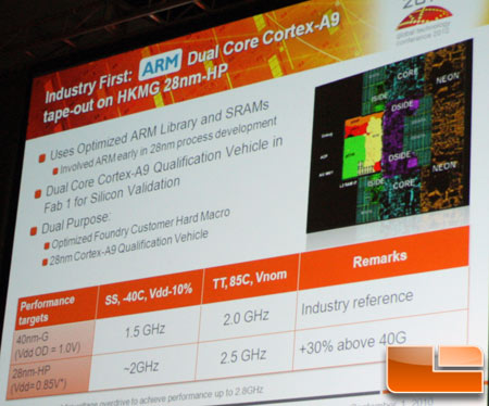
28HP in 2010 for ARM => 28SHP in 2014 for x86

With 28SHP being 2012.
28shp2012.png

40nm-G Cortex A9 (2009) -> 40nm-G Bobcat (2011)

22FDX in 2017 -> 22FDX+ in 2020; 22FDX+ uses the same PFET/NFET boosters as 12FDX which is from the 10FD node. << High Performance Strain Engineering on PMOS&NMOS Enabling Cost-Effective High Performance CPUs >>

Cost-crossover (Perf/Watt/$)
Geode LX 130nm = 2005
Bobcat 40nm = 2011
Stoney 28nm = 2017
22FDX = 2023

12FDX early cross-over needs JFIL for 56nm 1x pitch between M1-M8 to be competitive with the 28nm/22nm node.
Nothing new is coming from the Bulldozer line of CPUs and everything to say about them has already been said multiple times over.
It isn't Bulldozer, but more related to the older CMT designs at AMD: http://www.chip-architect.com/news/2001_10_02_Hammer_microarchitecture.html

Bobcat was developed against CMP cores. Jaguar was an IPC/Freq/SIMD-width improvement from Bobcat, but not a full new core.

2016-2018 for the CPU architect following Bobcat means that the ULP CPU Arch is 90% perf against SMT-core, rather than 90% perf against CMP-core. CMT is naturally the more dense threading IP. So, going forward the next-generation ULP core is 100% CMT.
sub1w.png

AMD design complete for Zen in 2015. AMD's ULP core design starts in 2016. Fully aware of Zen's performance to achieve 90% perf. It also explains off Stoney's bumping off Carrizo-L's successor Bristol-L. Since, the ULP core is between Fam 15h's CMT implementation and Fam 17h's SMT implementation.

Jaguar's logic area w/ CMT to cache area = 1.7 + 1.7 + 1.4 = 4.8 mm2
3.4 * ~0.7 + 1.4 * ~0.9 => 3.64 mm2 for same function unit throughput as Zen.
3.64+5.4(1 MB L2) + 3.64+5.4(1 MB L2) => 18.08 mm2 which is 4 mm2 less than 2c/4t Zen on 14LPP.

Less than$3600Less than$5400
Stoney 28BLKExcavator - 125 mm2Raven2 14LPPZen - 150 mm2
ULP SoC 22FDXULP Arch - 90 to 100 mm2Monet 12LP+Low-Cost Zen3 - >200 mm2
ULP SoC2 12FDXULP Arch2 - 75 to 90 mm2No successive nodeNo successive node
ULP SoC3 6FDXULP Arch3 - 60 to 75 mm2No successive nodeNo successive node
Market cap1 to 3 billion unitsMarket cap10 million to 20 million units


For example purposes;
Zen distribution w/o body-bias post-fab:
zendistribution.png
SS = 6W, TT = 15W, FF = 35W

ULP Arch distribution w/ body-bias post-fab:
ulparchdistribution.png
If 12W-25W becomes popular and has been analyzed for higher demand AMD can switch to FF-orientated bias increasing volume that way.

There is more DTCO options available with FDSOI over FinFET for maximum area, power, performance, cost, etc;
fdsoi.png
 
Last edited:
  • Like
Reactions: Tlh97 and Zepp

NTMBK

Lifer
Nov 14, 2011
10,237
5,019
136
Seriously, this thread needs to be closed. Nothing new is coming from the Bulldozer line of CPUs and everything to say about them has already been said multiple times over.

Nah, this thread will outlast us all. It's art.
 

amd6502

Senior member
Apr 21, 2017
971
360
136
NostaSeronx said:
Then, 22FDX is predominately aimed for small, cheap, monolithic chips like BRL&STR. Of which, AMD would max out cost-efficiency by inserting at the trailing edge;

If that were the case that would probably mean they would be porting some mystery GPU architecture to these nodes. Such architecture they would probably also license to other companies (which probably would be making products like risc-v or acorn family SoC's). What GPU architecture would be a good candidate for this? Would they have probems licensing (in the next few years) Navi because it's too leading edge?
 

NostaSeronx

Diamond Member
Sep 18, 2011
3,686
1,221
136
If that were the case that would probably mean they would be porting some mystery GPU architecture to these nodes. Such architecture they would probably also license to other companies (which probably would be making products like risc-v or acorn family SoC's). What GPU architecture would be a good candidate for this? Would they have probems licensing (in the next few years) Navi because it's too leading edge?
CPU = CMT-based with Linear IPC/power&area cores (Bobcat/Jaguar/Mongoose-esque)
GPU = Something in between CDNA(Compute/Tensor&Matrix) and RDNA(Gaming/Packed&Ray-tracing), with Tiny CUs/Small WGP.
Fabric = AMD Infinity Fabric
Multimedia = Cadence Xtensa+AMD?/HiFi 5
DDR&I/O = Cadence and/or Synopsys

What we are waiting for before AMD pulls the trigger:
1. 22FDX++ which uses new 12FDX transistors, FDX nodes are FEOL asymmetric. So, FEOL can be shared across BEOL nodes; (22FDX = 14FD FEOL, 22-28nm BEOL)
2. More modern variants of I/O-support; DDR5/LPDDR5/PCIE5/USB4 specifically from Synopsys
First launch 22FDX++ (DDR4) -> Second launch 22FDX+++ (DDR5), same die different transistors and enablement. Much like how Carrizo-variants were DDR3-orientated and Bristol-variants were DDR4-orientated. DDR4 is the most cost-efficient and most available currently, which might be held till 2024~2026.
3. 22FDX++ has to be available at Fab 1 and Fab 7, Sempron's home fabs;
sempronfabs.png
With Fab 8 as third source internal source.
Singapore + Pasir Ris = GloFo's biggest fab and SOITEC's biggest SOI wafer fab
Dresden + Bernin II = GloFo's second biggest fab and SOITEC's second biggest SOI wafer fab
Malta + St Peters = GloFo's smallest fab and GlobalWafer's local area SOI, unknown capacity for now.
SOITEC has a 3rd SOI fab in the works, and I expect given ~$4B+ wherever that fab is where GloFo will drop a 4th fab near it.

On one: 22FDX/22FDX+ = Lg20/14FD transistors w/ 22FDX being BOX20 and 22FDX+ being BOX15
22FDX++ = Lg15/10FD-12FDX transistors w/ 22FDX++ being strained BOX15 w/ 12FDX.

CTI path (like 90nm/65nm):
Node - Intro Year at Fab (not to customers)
22FDX - 2016 /Gen1
22FDX - 2017 /Gen2
22FDX - 2018 /Gen3
22FDX - 2019 /Gen4
22FDX+ - 2020 /Gen5
22FDX+ - 2021 /Gen6
22FDX++/12FDX - 2022 /Gen7
22FDX++/12FDX - 2023 /Gen8
22FDX moves away from logic improvement(if it was 90nm/65nm, but 22FDX/12FDX would be closely related in reality and continue at the same time)
12FDX - 2024 /Gen9
FDX is heavily CTI'd at GloFo similar to 90nm/65nm generation https://www.anandtech.com/show/2018
AMD enters at the end of logic improvement, rather at the beginning with the given trailing edge focus. Which gives highest performance&yield and lowest power&cost since it isn't intro-ing into a node when it is bad.

Assumptions;
CPU: CMT-Mode0 where replicating cores aren't a concern; Distributed, but shared Retire/Rename/PRF/Load-Store.
- Zen-like CMP-mode(Mode0p1), Zen-like SMT2-mode(Mode0p0), Excavator-like CMT2-mode(Mode1p0)
patentearlycmt.png
Rather than extra-wide monolithic structures, distributed less-wide structures are more efficient (maximize linear IPC-gain via replicated small-IPC superscalar pipeline structures)

GPU: Requirements probably need software work to be able to scale up to RDNA or CDNA. So compatibility to both is probably a need.
- G-series sells on CDNA-esque scale up, Sempron sells on RDNA-esque scale up.
CDNA-esque - Small-SIMD or Matrix Wavefront Compute => CDNAx Big-SIMD and Matrix Wavefront Compute,etc
RDNA-esque - Thinner Memories, Packed-SIMD Wavefront+RT Gaming => RDNAx Wider Memories, Packed-SIMD Wavefront+RT Gaming, etc

Everything else: Probably a requirement to support modern implementations, hence Infinity Fabric(rather than non-coherent Garlic and coherent Onion) and HiFi 5.
- Up to date system IP on-par with latest Zen SoC gen. <--- Minimal area gain, since Fixed Function has Fixed clocks, 22FDX-8T -> 22FDX++-6T at trailing edge implementation is a thing.

Node:
22FDX dev. cost is less than 14LPP/12LP+ for low ASP sub-$40 SoC (minus 30-40M$)
22FDX prod. cost is less than 14LPP/12LP+, ... (approximately minus 2000$ per wafer)
22FDX manufacturing capacity is heading multi-fab capable while 12LP+ is just Module 1 at Fab 8. (More fabs, less risk)
22FDX has more customers thus more IP options for semi-custom. (More customers, more markets to grow for semi-custom)

Exact-ish launch schedule based on a ray:
E2-9000e(2Q2017) -> 3015e(3Q2020)[reduced supply, reduced profit margin] -> 22FDX APU(4Q2023)
Which matches with named product launch ray:
Stoney(2016) -> Pollock(2020) -> 22FDX APU(2024)

Which gives AMD adequate time:
1. Strain SOI integration (+1.5 times freq, for unstrained 22FDX -> +2 times freq, for strained 22FDX)
2. Any 22FDX next-gen/plusplus w/ finer CPP and denser interconnect like Intel's 22FFL++ and Samsung's 17LPV.
3. If the ray goes on allows for 12FDX+ to go to a cost-reduced lithography: Late Standard-NA EUV(eliminate double patterning) or low-energy 6-cluster JFIL(more energy(fab-operation cost)/cost(tool-depreciation) efficiency). Which would go to the finer CPP and denser interconnect for 12FDX given 1Q27~2028.

There is also the semi-custom avenue being cheaper on the Geode/G-series lineup.
-> Wired router (OPNSense, PfSense)
-> Wireless router (OpenWRT)
-> Aerospace (re-design for Space-hard, and RISC-V to insert into Am29000-successor market)
-> Processor(22FDX)+FPGA(22FDX)

Allowing for a leapboard if successful to 6nm/4nm semi-custom
-> >4-port >10Gig wired
-> 16x16 WiFi 7/802.11be
-> ARM-premium (re-design for Space-tolerent)
etc

After calculating a bit(over several days) and guessing new titlenames based on Linkedin profiles;
Opteron Essentials => 4 modules; 4 CPU cores(SMT/CMP-mode) or 8 CPU cores(CMT-mode):: <$50USD, 9.9W TDP
Radeon Essentials => 384 32-bit ALU or equivalent:: <$50USD, 9.9W TDP
Sempron/G-series => 2 Modules, 192 32-bit ALUs or equivalent:: <$30 USD, 7.5W(SP1), 5W(SP2), ~3W(G1), ~1.5W(G2).

Reduced Die-cost
Reduced Package-cost
Reduced Systems-cost
Reduced Power-cost
etc.

====
Edit(April 2022): New GlobalFoundries stuff...

It is potentially a 3D Ultra-low-power SoC, numbers/stats above are somewhat accurate.

Stack-A: IODx (DDR5 PHY), CPUx(mid-die), CPUx(top-die) ==> Opteron Essential
Stack-B: IODy (LPDDR5 PHY), GPUx(mid-die), CPUx(top-die) ==> Sempron Essential
Stack-C: IODy (LPDDR5 PHY), GPUx(mid-die), GPUx(top-die) ==> Radeon Essential

Rather than a planar 100mm^2, it is likely to be a 50-75 mm2 with Z-height, etc.

12FDX is used for compatibility with 12LP-3D Logic/Logic process. As well as having the best density/performance given the price. With 12FDX being at least ~$1000 cheaper than 12LP/12LP+.
 
Last edited:
  • Love
Reactions: amd6502