NostaSeronx
Diamond Member
- Sep 18, 2011
- 3,815
- 1,294
- 136
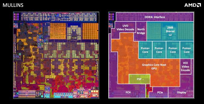
My sources implied;Bristol Ridge Refresh is not happening.
Heck, I see only AMD K12 using 22 nm.
- approximate 200 mm squared 22FDX replacing Vishera and targeted at Denverton/Jacobsville.
- approximate 150 mm squared 22FDX replacing both Bristol Ridge and Stoney Ridge, and targets at GLM+/JPL. (One die, multiple salvage slots; high FBB with low Vdd to low FBB with high Vdd to high FBB with high Vdd.) //high Vdd being 0.9V and low Vdd being 0.6V.
Both CPU and APU are AM4 compatible and the APU will be on FP5.
Vishera MSRP before EOL in 2017 was peaked at $130. So, the replacement at not salvaged should still be at $129. Bristol Ridge A8-9600 doesn't exceed $70. So, the successor at peak will not surpass that.
It is not expected that these processors will compete with any of the Zen/Zen+/Zen 2 SKUs. The platform is mainly aimed at providing features for low budget. So, performance is not a concern but power and cost is a concern.
Features (examples);
AVX512VL
AV1 L5.1? 12-bit? Encode/Decode
Follows Bristol Ridge as disguised Fire Pro, full half/double/quad precision speeds.
Speculation:
-> Zen2 Power/Area + FDSOI Intrinsic optimizations on top of Bristol/Stoney CPU.
-> Navi Power/Area + FDSOI """ on top of Bristol/Stoney GPU.
//Only two dimensions over each architecture. Power and area, with performance for the next node.
-> 22FDX Performance of Excavator/Puma, Enhanced Power/Area from Zen2.
2017 is an interesting year for AMD;
- AMD got a VISC person
- They invested in VISC
- Share patents with Intel.
I don't expect AMD to use Virtual Core or Soft ISA. Rather multi-core/module-orientated XVP and x86 ISA.
www.cs.cmu.edu/~seth/wild-and-crazy09/koreysewell.pdf
www.cs.cmu.edu/~seth/wild-and-crazy09/002-koreysewell.pptx
I'm slotting that for 12FDX models however. (If it is in 12FDX, then it will be in 3-nm. -> 12FDX Performance of Zen/Zen+, Enhanced Power/Area from Zen5.)
---
Extension edit:
Now the gritty details is that FBB/ABB has been significantly investigated.
So, Multi-FBB design does not increase area where Multi-Vdd does.
So, recompiling Excavator with a reduced Vdd design is going to drop its size. With Multi-FBB we are looking at max FBB up to 20x leakage and 5x increase in frequency.
A9-9420e is 2.6 GHz @ 1V~1.05V within a 6W TDP.
22FDX same design Excavator shrinks with a truncated Vdd. -> lower area
22FDX new design post-Excavator shrinks without that truncated Vdd. -> lower power
Math wise the 2.6 GHz @ ~1V on 28HPA becomes >2.6 GHz @ 0.9V on 22FDX. Now architecturally, the ideal is to get the same EPI as IPC from Zen. So, ~52% lower EPI for the new core. So, a 6W A9-9420e becomes a 3W part for 22FDX. The core with 20x the leakage and 5x the frequency is 60 watts and 13 GHz/13,000 MHz. This is just an example of max FBB, no one is ever going to do this ever. Except, maybe IBM or Oracle, the Z and M series from each are insane.
===
Edit for @Thunder 57
Nothing is final as of yet.GloFo is clearly using FD-SOI, I was curious as to anything AMD related it.
The expectation from myself is that it is inversion;
-> Jaguar evolves into Zen(17h/18h) a high performance core.
-> Excavator evolves into a new low-power and low-cost core(19h?).
AMD has been filter hiring from 2014 onwards, low power SoC/CPU-GPU RTL/Verification individuals. One major hire group is from STMicroelectronics.
For example, NovaThor L8580 eQuad(Dual-core A9 @ 3 GHz) which was followed in AMD with Stoney Ridge replacing Carrizo-L. A dual-core at faster clock rate replacing a quad-core or two bigger cores while running at lower energy. (ST-E NovaThor L8580 28FD Equad(Dual A9) vs Samsung Exynos 4412 Quad A9 and Exynos 5250 Dual A15)
There is plenty of architects that could have worked on low-power and low-cost design at AMD. There is a design and it should be substantially fast if the above is considered.
Zen started around 2012, and sampled late 2016.
The low-power and low-cost core should have started around 2014. So, if following the above it should sample late 2018.
Zen sampled to the public in 2016 -> https://techreport.com/review/30540/amd-gives-us-our-first-real-moment-of-zen
Early, I commented Atari VCS might be the one. Following the pattern of above then...
https://c1.iggcdn.com/indiegogo-med...it,w_695/v1527637991/pzuaczs9wvmx4n7pfx70.jpg
...the Atari VCS could possibly be the first to use the LP/LC core.
https://www.theregister.co.uk/2018/06/21/atari_interview_in_full/
https://regmedia.co.uk/2018/06/20/atari-chip.mp3 <-- For example.
Utilizing a new chip on FDX, is more cost-effective than using FinFET chips.
https://www.anandtech.com/show/1243...ew-with-dr-gary-patton-cto-of-globalfoundries <== quotes from this guy.
- 22FDX will be a long-lived node so I expect will retrofit many technology modules
- We have been doing work on 12FDX here in NY for over a year .... We expect to be taking risk production on the parts early next year (2019), so we are pretty far along with the technology.
- We expect tape outs on 12FDX in 2020 with deliveries in 2021.
/ End quotes from GP.
22FDX thus tapes out in 2018, delivers in 2019. With the above information.
Last edited: