
News AMD Announces Radeon VII
Page 14 - Seeking answers? Join the AnandTech community: where nearly half-a-million members share solutions and discuss the latest tech.
You are using an out of date browser. It may not display this or other websites correctly.
You should upgrade or use an alternative browser.
You should upgrade or use an alternative browser.
Nah. Since the 2080 was launched in Sep I doubt we'll see 7nm GPU's for consumer from Nvidia this year. There were rumours only a few weeks ago that Nvidia will use Samsung's 7nm EUV for it's next-gen 7nm GPU's. Makes sense tbh since it would be weird to launch 7nm GPU's in like Q4 2019 if you instead can launch your GPU's on 7nm EUV in the first half of 2020.Not sure. By July Nvidia should be only a few months away from launching their own 7nm since the 2080 was launched Sep-Oct
beginner99
Diamond Member
- Jun 2, 2009
- 5,320
- 1,768
- 136
Nah. Since the 2080 was launched in Sep I doubt we'll see 7nm GPU's for consumer from Nvidia this year.
Agree. General take away is: It's a bad time to upgrade your GPU. Better to wait for new uArch on 7nm and even for AMD I suspect Navi will be Q1 2020.
PeterScott
Platinum Member
- Jul 7, 2017
- 2,605
- 1,540
- 136
Nah. Since the 2080 was launched in Sep I doubt we'll see 7nm GPU's for consumer from Nvidia this year. There were rumours only a few weeks ago that Nvidia will use Samsung's 7nm EUV for it's next-gen 7nm GPU's. Makes sense tbh since it would be weird to launch 7nm GPU's in like Q4 2019 if you instead can launch your GPU's on 7nm EUV in the first half of 2020.
I don't know about rumor, but I agree that we won't see much 7nm action from NVidia this year.
I remember when Turing launched on 7nm a whole bunch of people here said was a temporary stopgap and we would see 7nm Nvidia cards in 6-9 months, which is just nonsense.
Maybe if it were one chip, but NVidia has a whole range of chips, you don't do that many tapeouts to throw them away in less than a year.
Nvidia is committed to a full "12nm" release, and it will likely run through all of 2019.
This also give NVidia time to pick the best, most mature 7nm process for it's next generation, after it has matured.
This does give AMD an opening with it's mid-range 7nm cards, but process isn't everything. Vega didn't really benefit that much from the shrink. It will really be more about how much improved Navi architecture is.
What do you mean it hasn't? Have you seen how many transistors they can pack in a smaller package AND increase clock speeds at the same voltage?I don't know about rumor, but I agree that we won't see much 7nm action from NVidia this year.
I remember when Turing launched on 7nm a whole bunch of people here said was a temporary stopgap and we would see 7nm Nvidia cards in 6-9 months, which is just nonsense.
Maybe if it were one chip, but NVidia has a whole range of chips, you don't do that many tapeouts to throw them away in less than a year.
Nvidia is committed to a full "12nm" release, and it will likely run through all of 2019.
This also give NVidia time to pick the best, most mature 7nm process for it's next generation, after it has matured.
This does give AMD an opening with it's mid-range 7nm cards, but process isn't everything. Vega didn't really benefit that much from the shrink. It will really be more about how much improved Navi architecture is.
The biggest thing they are getting is more transistors in a smaller die that performs better at the same wattage levels. That is huge!
Radeon 7 is much smaller than Vega 64, much higher clock speeds at the same wattage. Coupled with some smaller tweaks to the architecture it performs faster clock for clock than the Vega 64.
Specs from Sapphire's product page:
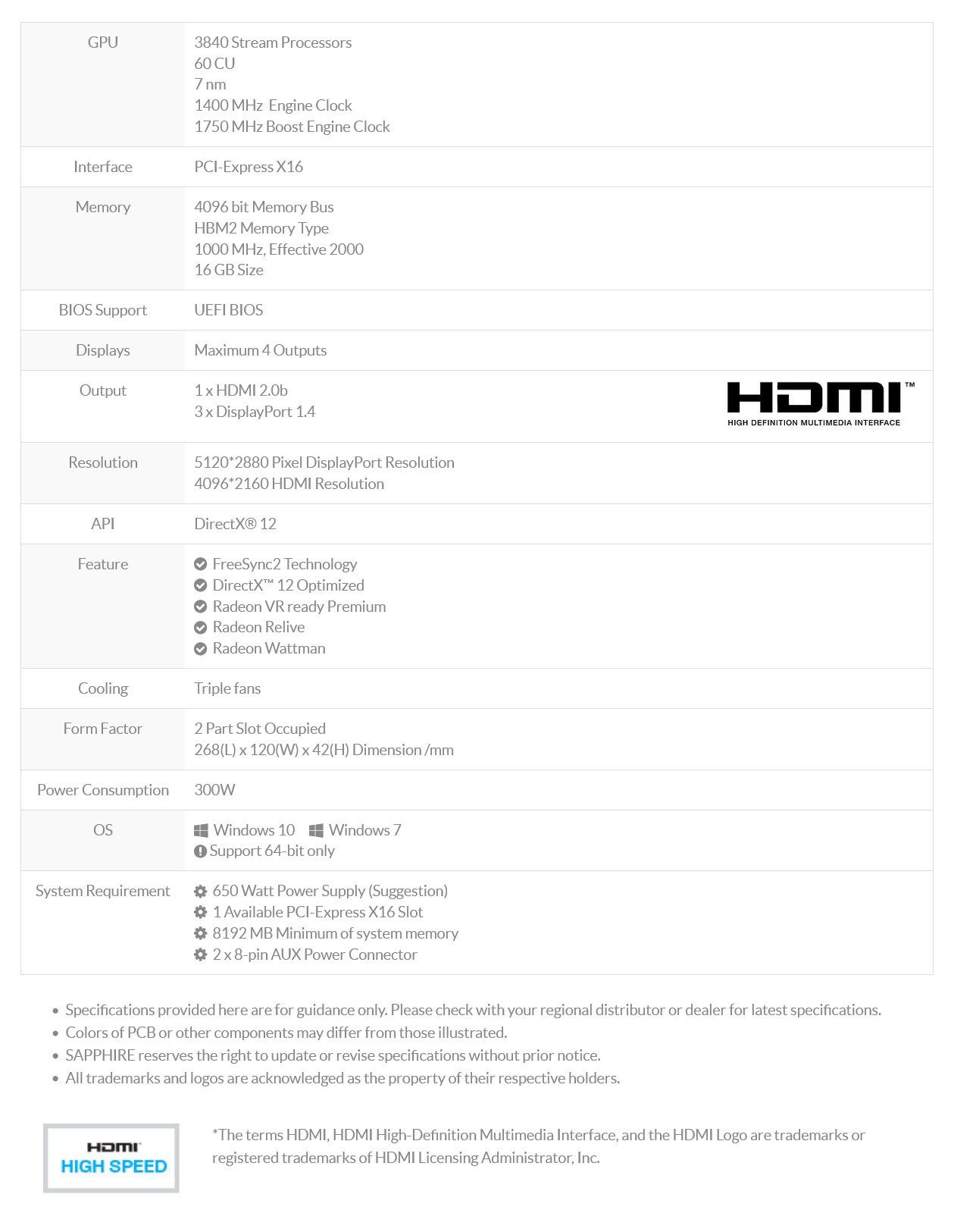
http://www.sapphiretech.com/productdetial.asp?pid=97FA4A9F-D64C-45E6-A0C4-B8911A7EE2B3&lang=eng
http://www.sapphiretech.com/productdetial.asp?pid=97FA4A9F-D64C-45E6-A0C4-B8911A7EE2B3&lang=eng
What do you mean it hasn't? Have you seen how many transistors they can pack in a smaller package AND increase clock speeds at the same voltage?
The biggest thing they are getting is more transistors in a smaller die that performs better at the same wattage levels. That is huge!
Radeon 7 is much smaller than Vega 64, much higher clock speeds at the same wattage. Coupled with some smaller tweaks to the architecture it performs faster clock for clock than the Vega 64.
It isn't as big of a difference as you make it out to be. The die is ~330 mm^2 down from ~490 mm^2, but TSMC's 7 nm wafers are estimated to be at least double (if not more) the price, so AMD isn't realizing any significant cost savings.
The clock speeds are less than a 10% bump for both base and boost clock (Edit: I used the Vega 64 Liquid clocks, so compared to the base Vega 64, it's slightly better), so there isn't much of a jump there either. Most of the changes to the core design were for compute and machine learning workloads, not gaming performance.
There's nothing huge about this card. Unless you consider the letdown.
Last edited:
LTC8K6
Lifer
- Mar 10, 2004
- 28,520
- 1,576
- 126
That's less SPs than Vega 64 though with presumably the same GCN5.3840 stream processors. Thats cuda cores, right ? If its at $799, I may have to get one.
PeterScott
Platinum Member
- Jul 7, 2017
- 2,605
- 1,540
- 136
The clock speeds are less than a 10% bump for both base and boost clock, so there isn't much of a jump there either. Most of the changes to the core design were for compute and machine learning workloads, not gaming performance.
And some of the performance may be attributed to the big jump in Memory Bandwidth, which is nothing to do with process.
That is a 160mm difference, what are you talking about? That is an entry sized chip like a GTX 1050 or RX 560, heck even a bit more. GTX 1060 is 200mm, that is just 40mm more.It isn't as big of a difference as you make it out to be. The die is ~330 mm^2 down from ~490 mm^2, but TSMC's 7 nm wafers are estimated to be at least double (if not more) the price, so AMD isn't realizing any significant cost savings.
The clock speeds are less than a 10% bump for both base and boost clock, so there isn't much of a jump there either. Most of the changes to the core design were for compute and machine learning workloads, not gaming performance.
There's nothing huge about this card. Unless you consider the letdown.
https://www.anandtech.com/show/13445/tsmc-first-7nm-euv-chips-taped-out-5nm-risk-in-q2
Second we don't know the costs of 7nm, yeah it's probably higher, but by how much? If it's say 40% higher price, but offers 60% more die area, than that is a win for AMD and as the process manufacturing ramps up and becomes more mature, it becomes cheaper and cheaper and more economical.
And clock speeds are about 15-20% higher.
That is a 160mm difference, what are you talking about? That is an entry sized chip like a GTX 1050 or RX 560, heck even a bit more. GTX 1060 is 200mm, that is just 40mm more.
It doesn't really matter as much as you think it does. AMD only gets about ~45% more dies per wafer, around 50 or so dies. However, because the 7nm process isn't as mature, They may not get all that many more fully functional dies.
Additionally, if you use a lot of that space for compute hardware, it doesn't add much performance for gaming.
Second we don't know the costs of 7nm, yeah it's probably higher, but by how much? If it's say 40% higher price, but offers 60% more die area, than that is a win for AMD and as the process manufacturing ramps up and becomes more mature, it becomes cheaper and cheaper and more economical.
Most information puts the costs at the bare minimum as twice as much, possibly higher. It will eventually come down, but it's still a new node and other companies like Apple buy a lot of wafers.
There's no cost advantage, which is part of the reason (the extra HBM doesn't help) than Radeon VII is more expensive than Vega 64 was.
And clock speeds are about 15-20% higher.
They're not quite that good, though apparently when I gave some numbers earlier, I used the numbers for Vega 64 Liquid, so they're a little bit better than I originally thought, at least if you're comparing it to Vega 64.
Vega just didn't work out for a lot of various reasons and had you told me 3 months ago that this is what AMD was going to have, I would have not had any hopes for it.
piesquared
Golden Member
- Oct 16, 2006
- 1,651
- 473
- 136
What do you mean it hasn't? Have you seen how many transistors they can pack in a smaller package AND increase clock speeds at the same voltage?
The biggest thing they are getting is more transistors in a smaller die that performs better at the same wattage levels. That is huge!
Radeon 7 is much smaller than Vega 64, much higher clock speeds at the same wattage. Coupled with some smaller tweaks to the architecture it performs faster clock for clock than the Vega 64.
Agreed, Radeon 7 seems to he a big performance increase over last gen. "Clock speeds don't appear to be significantly increased though, so the architecture has gained a large portion of the performance, even with 4 fewer CUs! The 330mm 7nm die's competing product is 529mm. Crazy that nvidia wasted space on that ray tracing luggage that is for all intents and purposes, useless.
GodisanAtheist
Diamond Member
- Nov 16, 2006
- 8,494
- 9,922
- 136
Agreed, Radeon 7 seems to he a big performance increase over last gen. "Clock speeds don't appear to be significantly increased though, so the architecture has gained a large portion of the performance, even with 4 fewer CUs! The 330mm 7nm die's competing product is 529mm. Crazy that nvidia wasted space on that ray tracing luggage that is for all intents and purposes, useless.
- I am really curious to see how these reviews pan out. Where is this supposed 25-30% performance increase coming from?
Maybe it's just sustained boost clocks, maybe AMD got some of their secret sauce working... We'll find out soon enough.
Stuka87
Diamond Member
- Dec 10, 2010
- 6,240
- 2,559
- 136
Process shrinks just aren’t magic anymoreThere’s stuff to be gained but it takes genuinely hard work to get it!
Process shrinks stopped being true shrinks years ago. Chips are smaller for sure, and you still are able to put more transistors in a given place. The number now just means more of a process change, rather than an actual node shrink. But also the changes aren't to the same degree as they once were. Like going from 65nm down to 40nm was a gigantic difference as it was an actual node shrink. 14nm to 7nm may sound like the node shrank by 50%, but in reality it didn't.
Stuka87
Diamond Member
- Dec 10, 2010
- 6,240
- 2,559
- 136
I dont know what you are talking about but 7nm TSMC gave 58% higher density and 50% lower power at iso perf over GloFo 14nm.
Vega 10 = 12.5B transistors at 495mm2
Vega 20 = 13.23B transistors at 331mm2
Its hard to compare processes across different fabs, as just because the process is called something similar, doesn't mean they are. The transistors in many cases are different, which has an impact on the size of the chip with X number of transistors.
The drop from 20nm to 16nm actually had NO change to the node at all. The only change was in the transistor design (they switched to finFETs). TSMC changed the name to signify that they could now fit 20% more transistors on the same size chip.
14nm is Samsung/GloFlo's finFET version of 20nm chips
You then also have 10nm and 7nm. These names are done to signify differences in the process, which does allow for more transistors, but are typically a result of different types of transistors (fitFET, Triangle, etc). Not node shrinks.
Krteq
Golden Member
- May 22, 2015
- 1,010
- 730
- 136
Interesting. XFX stated 1801MHz as a "Peak" clockSpecs from Sapphire's product page:
http://www.sapphiretech.com/productdetial.asp?pid=97FA4A9F-D64C-45E6-A0C4-B8911A7EE2B3&lang=eng
XFX Radeon VII 16GB 4096 Bit HBM2, DX12 VR Ready, Triple Fan, 3xDP HDMI, PCI-E AMD Graphics Card (RX-VEGMA3FD6)GPU ClockBase: 1400MHz, Boost: 1750MHz, Peak: 1801MHz
And some of the performance may be attributed to the big jump in Memory Bandwidth, which is nothing to do with process.
Vega 64 already had pretty good memory bandwidth (around the same amount as a 1080 Ti) so I'm not sure how much Radeon VII gains from added bandwidth. I know that NVidia added some better compression in Pascal that made their bandwidth more effective, but AMD wasn't that far off.
Given everything else we know about Vega (and GCN in general) I'd be surprised if memory was the bottleneck in most situations.
XFR?
Seems unlikely or AMD would have talked about bringing the feature to their GPUs. The XFX page is down (I get a 404) so I'm not too sure what the deal is. I'd have to go back to watch the keynote to see if AMD said something like "up to 1800 MHz boost" where it's not guaranteed.
darkswordsman17
Lifer
- Mar 11, 2004
- 23,444
- 5,852
- 146
- I am really curious to see how these reviews pan out. Where is this supposed 25-30% performance increase coming from?
Maybe it's just sustained boost clocks, maybe AMD got some of their secret sauce working... We'll find out soon enough.
Likely from doubling the memory bandwidth. There was some analysis of memory bandwidth and I think they found that doubling it generally can bring ~25% performance improvement on its own (for GPU related tasks). Some variance and its possible that particularly memory bound situations would benefit more. 16GB of 1TB/s memory would be awesome for very high quality texture assets (there was speculation that games might look to that as a way of pushing quality forward, where they'd pair it with like more advanced bump mapping as a way of making it look like more complex model but using less geometry - and therefore offering higher quality on lower end GPUs; I actually think that was maybe AMD's aim, and why they let their geometry throughput languish thinking that HBM would let them push bandwidth and possibly memory capacity to where that would be possible; I believe that was what AMD's Tessellation stuff was about early on, it was like a way of taking bump mapping to the next level, and when paired with adequate textures wouldn't need GPUs to scale as much in geometry and since higher quality textures were already being called for, that it might be a way of making things look especially good ; Rage I think was kinda designed around accomplishing something like that as well, and integrating the textures so that it would help remove edges and other things that would disrupt a coherent image; and I think it would make culling more effective too, since textures would hide a lot).
Due to AMD's history, I won't be surprised to find that people will be able to drop voltage and get power down to 250 or even closer to 200 W with little impact to performance (maybe drop clock speeds a bit), and possibly even improve it over the course of gaming (by it enabling it to hold higher clocks for longer periods). Will be curious to see if people might be able to overclock and get close to 2GHz (at stock or close to stock voltage) using watercooling.
I absolutely don't expect it, but if people are able to drop voltage and overclock, this might turn out to be a pretty decent gamer card after all. Still not something I'd buy, but would make it more appealing for those that would, and that should enable it to hit 4K at solid framerates.
Ugh, too bad they're gimping it with HDMI 2.0. This card would be a lot more appealing with HDMI 2.1 as at least it'd offer something for people that will buy HDMI 2.1 display this year, and would help it with 4K and Freesync/VRR capable stuff.
Also, why are they sticking with 3 DP connectors? I could see one, and one HDMI, but they could've had 4 miniDP or even better USB-C (displayport) capable ports instead of 3 DP (and mini-DP to DP doesn't need anything crazy for adapters does it? So just include at least one adapter). I absolutely hate this particular layout though (my reference RX 480 has it, and I've had to get multiple cables/adapters because I didn't have any DP monitors, I did have a miniDP to HDMI cable from when I had a Surface Book though; mine was made a bit worse since I'm currently stuck using two monitors with DVI after my HDMI one burnt a cap or something). I'd prefer 2DP and 2HDMI even.
I hope I'm not gonna find it impossible to get a video card with 2 HDMI 2.1 connectors (and whatever beyond that, although that with a couple of USB C 3.1/Thunderbolt 3 connectors would be optimal for me) anytime soon. I wish they'd break the I/O ports out (so you could adjust where they are, and it'd free up the slots for venting heat from the GPU). Some used to do that (like the half height cards), and it'd allow more flexibility so you could get what ports you need. You could swap out the port selection (or keep what ones you have already). It would help for stuff like transitions to new port specs (HDMI/DP, etc) as well. And with it looking like USB-C Thunderbolt will become a popular one, and it needing more power, it having its own PCIe slot and separate power would benefit GPUs, where their boards won't need to be tasked with that extra draw.
I'm hoping AMD integrates some manner of display controllers in the I/O part of Ryzen, so that you could use motherboard display I/O with or without an actual GPU (so you could get video decode/encode, GUI handling, you just wouldn't be able to game). And it would mean your ports wouldn't go to waste there).
Ugh, too bad they're gimping it with HDMI 2.0. This card would be a lot more appealing with HDMI 2.1 as at least it'd offer something for people that will buy HDMI 2.1 display this year, and would help it with 4K and Freesync/VRR capable stuff.
LOL, I hate when companies do that. They always cut off some corner of something from making it 100% perfect. My Canon camera is USB 3.0 and accepts CF and SD memory slots, but they gimped the SD protocol and could have had a faster SD for faster speed.
AtenRa
Lifer
- Feb 2, 2009
- 14,003
- 3,362
- 136
Its hard to compare processes across different fabs, as just because the process is called something similar, doesn't mean they are. The transistors in many cases are different, which has an impact on the size of the chip with X number of transistors.
The drop from 20nm to 16nm actually had NO change to the node at all. The only change was in the transistor design (they switched to finFETs). TSMC changed the name to signify that they could now fit 20% more transistors on the same size chip.
14nm is Samsung/GloFlo's finFET version of 20nm chips
You then also have 10nm and 7nm. These names are done to signify differences in the process, which does allow for more transistors, but are typically a result of different types of transistors (fitFET, Triangle, etc). Not node shrinks.
According to TSMC
https://www.tsmc.com/english/dedicatedFoundry/technology/16nm.htm
TSMC’s 16/12nm provides the best performance among the industry’s 16/14nm offerings. Compared to TSMC’s 20nm SoC process, 16/12nm is 50 % faster and consumes 60% less power at the same speed. It provides superior performance and power consumption advantage for next generation high-end mobile computing, network communication, consumer and automotive electronic applications.
Also for 7nm ,
https://www.tsmc.com/english/dedicatedFoundry/technology/7nm.htm
Compared to its 10nm FinFET process, TSMC’s 7nm FinFET features 1.6X logic density, ~20% speed improvement, and ~40% power reduction. TSMC set another industry record by launching two separate 7nm FinFET tracks: one optimized for mobile applications, the other for high performance computing applications.
- I am really curious to see how these reviews pan out. Where is this supposed 25-30% performance increase coming from?
Maybe it's just sustained boost clocks, maybe AMD got some of their secret sauce working... We'll find out soon enough.
Yeaa this is some weird situation and I agree they need something extra to reach 2080..
If we take Lisa explanation that this gpu was also intended for gaming at face value and I think we can do that - It's weird if they didn't use those extra b of transistor and 300m takeout to fix those parts of the design that made the ngg path broken.
They had their time.
I guess most is software cost but still. An entire arch is basically laying dormant in Vegas acting like Hawaii with a speed bump. Its clumsy and costly at the same time as it looks now.
I hope they got it to work on the driver side now. Fingers crossed !
TRENDING THREADS
-
 Discussion Zen 5 Speculation (EPYC Turin and Strix Point/Granite Ridge - Ryzen 9000)
- Started by DisEnchantment
- Replies: 25K
-
Discussion Intel Meteor, Arrow, Lunar & Panther Lakes + WCL Discussion Threads
- Started by Tigerick
- Replies: 24K
-
 Discussion Intel current and future Lakes & Rapids thread
- Started by TheF34RChannel
- Replies: 23K
-

-

AnandTech is part of Future plc, an international media group and leading digital publisher. Visit our corporate site.
© Future Publishing Limited Quay House, The Ambury, Bath BA1 1UA. All rights reserved. England and Wales company registration number 2008885.