Question AM5 number of pins vs AM4? (1718 vs 1331)

Kedas

Senior member
Dec 6, 2018
355
339
136
So what are we going to use the extra pins for? (387 pins)

If we assume (I don't know) that 2/3 are power supply pins on AM4 and AM5 increase power to 120W from 105W then we need about 130 extra pins.
(feel free to count https://www.docdroid.net/6cDW11N/am4-pinout-diagram-pdf)

Still about 250 left.

The number of pins for the DDR interface is about the same I think (DDR4 vs DRR5)
PCI-E 5 they can add more lanes let say 32 extra pins.
A few more USB lets say 20 extra pins.

So still more than half left of the new extra pins?
(I assume they don't add more than 200 pins just not to use them.)

Maybe even higher TDP 140W...(that would use up all pins)
 

Tuna-Fish

Golden Member
Mar 4, 2011
1,358
1,567
136
If we assume (I don't know) that 2/3 are power supply pins on AM4 and AM5 increase power to 120W from 105W then we need about 130 extra pins.
(feel free to count https://www.docdroid.net/6cDW11N/am4-pinout-diagram-pdf)

You need more than that. The amount of pins needed for power supply does not depend on the power that flows through them, but the current. Or, amperes, not watts. This is a problem because new CPUs will have lower voltages, and current is power/voltage. And you also need to match the increased power pins with a similar amount of new ground pins. I think that's almost all of the increase right there.

This is why Intel's FIVR is such a desirable technology despite it's downsides. It allows pushing the voltages that come into the socket up, which means less pins you have to waste on power/ground.
 

Kedas

Senior member
Dec 6, 2018
355
339
136
True but I assume the voltage won't change much between 7nm and 5nm AMD CPU's
The new ground pins are part of the extra 130pins. (just like ground pins are also part of '2/3 are power supply pins')
 

leoneazzurro

Senior member
Jul 26, 2016
935
1,482
136
IIRC; in the leaked documents from Gigabyte there were indications that on AM5 there will be up to 170W parts even if probably first supported CPU/APU will be lower than that.. So this could be a further explanation for these added pins.
 

NostaSeronx

Diamond Member
Sep 18, 2011
3,687
1,222
136
This is why Intel's FIVR is such a desirable technology despite it's downsides. It allows pushing the voltages that come into the socket up, which means less pins you have to waste on power/ground.
FIVR is also more efficient across the board. 12V to 1.8V + 1.8V to 1.0V is more efficient than 12V to 1V. Despite the downsides it means less power is released as waste overall.

When FIVR was introduced majority of systems were 65% efficient, while the FIVR system was ~85% efficient.
 
Last edited:

JoeRambo

Golden Member
Jun 13, 2013
1,814
2,105
136
FIVR is also more efficient across the board. 12V to 1.8V + 1.8V to 1.0V is more efficient than 12V to 1V. Despite the downsides it means less power is released as waste overall.

I think during Intel's desktop FIVR era ( Haswell + Broadwell ) the problemas was the following: the power dissipated in 12V => 1.2V system is in VRMs and power stages of motherboard and does not add up to CPU TDP.
With FIVR, even if it is very efficient and fed 1.8V to convert 1.2V, every watt lost due to converssion inneficiencies eats into CPU TDP and cooling requirements.


NostaSeronx

Diamond Member
Sep 18, 2011
3,687
1,222
136
I think during Intel's desktop FIVR era ( Haswell + Broadwell ) the problemas was the following: the power dissipated in 12V => 1.2V system is in VRMs and power stages of motherboard and does not add up to CPU TDP.
With FIVR, even if it is very efficient and fed 1.8V to convert 1.2V, every watt lost due to converssion inneficiencies eats into CPU TDP and cooling requirements.
PGT Loss is included into TDP, but only at highest Vout where it was most efficient. If it was lower, then the processor wasn't at full blast or at TDP anyway basically eating the extra heat.

$60 basic VRM mobo <-> $150 higher-end VRM => same ~85% efficiency but if it was IVB it was ~65% on basic warranting the high-end VRM. In this case, the consumer has $90 for cooling if need be, before HSW one core couldn't hog a Vrail. The best cases were mobile and server, though platform power and area loss is a huge budget for them. It also allowed them to push out the 5x5 concept/Mini-STX sooner than later. Server-side platform power w/o FIVR >175W, w/ FIVR <150W for 145W processor.

Using pixel measurement:
serverhaswellpower.png
It allowed power to actually be below TDP which is the orange line. Red line is power/heat from FIVR system and clipped purple line is w/o FIVR system.
 
Last edited:

Bigos

Member
Jun 2, 2019
131
295
136
The number of pins for the DDR interface is about the same I think (DDR4 vs DRR5)

Don't forget that DDR5 channels are twice as small, so there might be some additional overhead with supporting 4 (32-bit) instead of 2 (64-bit) channels.

One such overhead is ECC, which adds 8 additional bits per channel. So on AM4 there were 144 bits (2 x (64 + 8)) while on AM5 there will be 160 bits (4 x (32 + 8)).

Unless AMD completely removes ECC support from their consumer socket, which is unlikely.
 

Kedas

Senior member
Dec 6, 2018
355
339
136
Last edited:

Mopetar

Diamond Member
Jan 31, 2011
7,885
6,136
136
They may have some left unused and reserved for future needs/use. AM4 stuck around for a while and it's difficult to imagine that AMD didn't run into a few issues with later AM4 products. AMD did have to bend with Threadripper and release a new socket and may have learned from that. Also they may be planning it around what Zen 5 and future chips bring to the table and not just what they'll need for Zen 4.
 

zir_blazer

Golden Member
Jun 6, 2013
1,167
410
136
They may have some left unused and reserved for future needs/use. AM4 stuck around for a while and it's difficult to imagine that AMD didn't run into a few issues with later AM4 products. AMD did have to bend with Threadripper and release a new socket and may have learned from that. Also they may be planning it around what Zen 5 and future chips bring to the table and not just what they'll need for Zen 4.
Makes me remember than the Intel Xeon Scalable LGA 3647 used to expose only 48 PCIe Lanes then expanded them to 64 on the 1P Xeon W 3200 series.

AM4 actually lacks Pins - I have ranted A LOT about AMD not exposing the entire 32 PCIe Lanes of original Zeppelin instead of only 24.
 
  • Like
Reactions: Tlh97 and Joe NYC

Tuna-Fish

Golden Member
Mar 4, 2011
1,358
1,567
136
True but I assume the voltage won't change much between 7nm and 5nm AMD CPU's

1. It will.
2. A large part of the success of AM4 has been that it's had much more compatibility, both forward and backward, than the Intel alternatives. This means that it's not sufficient to just design the socket to support TSMC 5nm, they need to support whatever voltages the last AM5 CPU (which will hopefully be the last AMD DDR5 cpu) needs.
 

jamescox

Senior member
Nov 11, 2009
637
1,103
136
Yes they did change the DDR data lines 72 bit (1*40+32) to 80 bit (2*40) but they also rearranged other parts to end up with the same number of connections.
You can see that here: https://prog.world/ddr5-memory-specs-released/
DDR4 pin-out https://sector.biz.ua/docs/pinouts_desktop_ddr4_memory/ddr4_1_pins.jpg

The many 'power' pins here are not for max current reasons but for signal quality protection.

It goes from 32 data + 40 data + 24 cmd bus to 40 data + 40 data + 7 cmd bus + 7 cmd bus.


Specifically the image here:

It would be nice if AM5 is triple channel capable for future zen 5 cores that may take a lot more memory bandwidth, but I don’t know if they have sufficient pins to go more than dual channel. They can use on die HBM or just massive SRAM caches, I guess.
 
  • Like
Reactions: Tlh97 and Joe NYC

zir_blazer

Golden Member
Jun 6, 2013
1,167
410
136
They're there. Just used for other things. 4 for SATA and 4 for USB3.
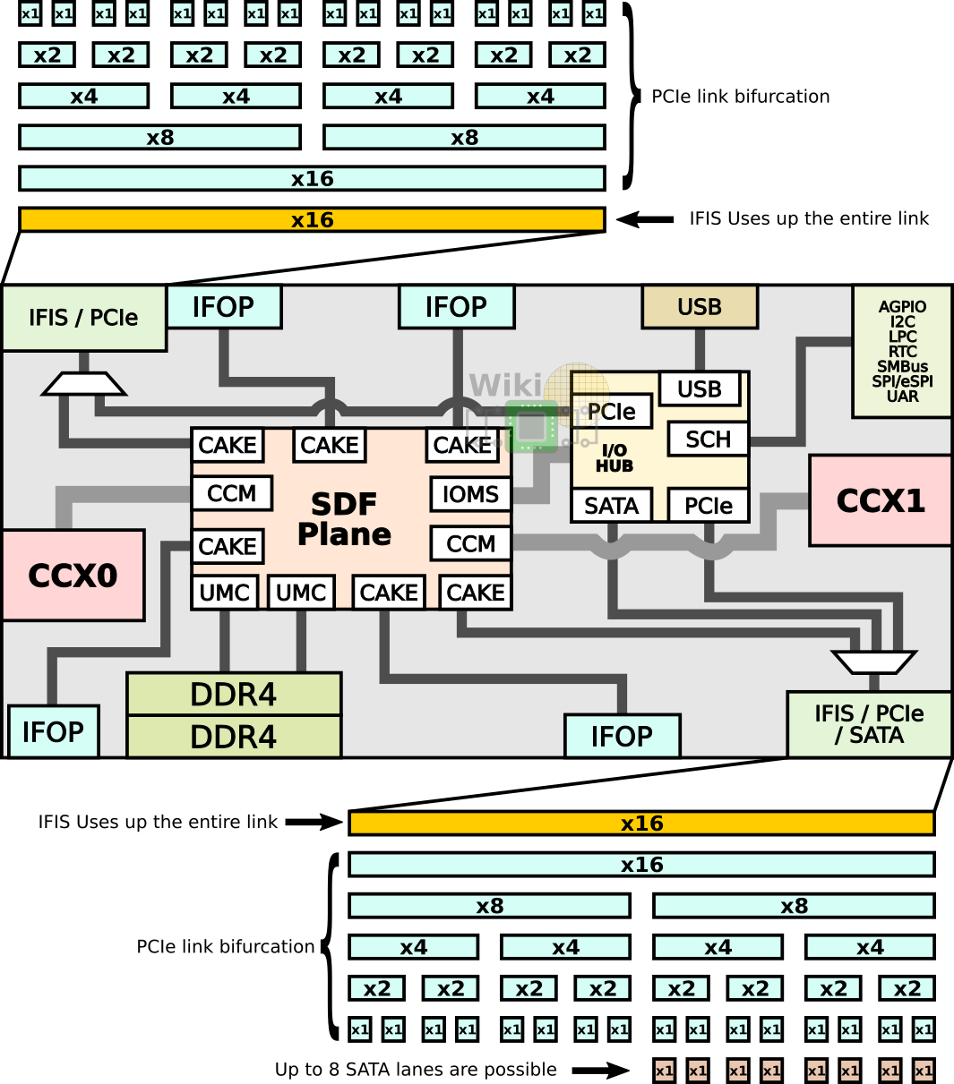
Nope. Zeppelin has a total of 32 PCIe Lanes, of which 8 are also multiplexed to SATA, so that you could theorically do 24 PCIe Lanes + 8 SATA. AM4 exposes a total of 24 PCIe Lanes, and only TWO of those are SATA (It is unknow to me if the 4 lanes typically used by the Chipset could be set to SATA, assuming that you're using an A300/X300 "Chipset", in which case you have a total of 24 usable PCIe Lanes, of which 6 can be setup as SATA).
The 4 USB Ports are dedicated, they're not shared with anything. Is not like Flex IO on some Intel Chipsets where you have a choice of USB or PCIe on a configurable Port.

I did a Thread about that some years ago.

I'mt not sure about if anything after Zeppelin (Like Zen 2/3 IO die) supports that too or AMD trimmed the I/O to match the Socket capabilities, since you have cases like Renoir or Cezanne that seems to be 24 PCIe Lanes on the die instead of 32 like on the first Zen.
 
Last edited:

Insert_Nickname

Diamond Member
May 6, 2012
4,971
1,691
136
Is not like Flex IO on some Intel Chipsets where you have a choice of USB or PCIe on a configurable Port.

Don't know where you got that info, because that's exactly what it is. Zeppelin has 32 lanes, but only the second root complex is flexible in what it can be configured as. There is even a diagram showing this, but I can't find it. It's buried somewhere in the early Zen threads.

Edit; found it:


zeppelin-block-mux.png


You're correct. The USB is indeed separate. My bad. :)
 
Last edited:

zir_blazer

Golden Member
Jun 6, 2013
1,167
410
136
You're correct. The USB is indeed separate. My bad. :)
Fun fact: That diagram predates EPYC Embedded, so is missing Zeppelin 4 10G MACs (10GBASE-KR). Before EPYC Embedded, the existence of these was completely unknow. Since there was no new diagram including these, it was never explained how these MACs were exposed, but after looking at EPYC Embedded industrial boards Block Diagrams like the SECO COMe-C42-BT7, it became evident than these were multiplexed onto 4 of the PCIe Lanes that could also do SATA (At some point I thought that a pair of lanes were teamed to provide the bandwidth so 4 MACs took a 8 lane budget, but it seems that they're actually individual). The diagram of that Motherboard looks like this:

SerDes Port 0-1 (2) ---------- 2x SATA exposed on COM Express Connector
SerDes Port 2 (1) ------------- 1 PCIe Lane for NIC onboard the COM Express Module
SerDes Port 3 (1) ------------- Not Connected probably
SerDes Port 4-7 (4) ---------- 4x 10GBASE-KR exposed on COM Express Connector
SerDes Port 8-13 (6) -------- 6 PCIe Lanes exposed on COM Express Connector
SerDes Port 14-15 (2) ------ 2 PCIe Lanes exposed on COM Express Connector
SerDes Port 16-31 (16) ---- 16 PCIe Lanes exposed on COM Express Connector
TOTAL 32 Ports. 24 are pure PCIe, 4 are PCIe or SATA, and 4 are PCIe or SATA or 10GBASE-KR

USB SS Port 0-3 (4) ------------- 4 USB 3 Ports exposed on COM Express Connector
USB 2.0 Port 0-3 (4) ------------ These seem to be the same as above
TOTAL 4

The inclusion of the 4 10GBASE-KR MACs should be because that is a major feature of the COM Express Type 7 specification. Do note that in theory the connector should expose 32 PCIe Lanes + 4 10GBASE-KR + 2 SATA + 4 USB 3.0 + 4 USB 2.0 + NIC, but EPYC Embedded doesn't deliver all that. Nor Xeon D, actually, which is its competitor on that space.

Yeah, I'm still bitter about AMD not fully exploiting all what already was in silicon. Maybe AM4 didn't expose all that because it would force every other Processor to include as much I/O respecting the exact same pinout and Flex IO configuration, because otherwise you will have half the Motherboard dead if you put a low end APU or something (Remember Kaby Lake-X?).
 
Last edited:
  • Like
Reactions: Tlh97 and scineram