Good point. I am no expert on this. I have read some articles about
wafer testing (probing) and
known-good-die (KGD) schemes, in which it is stated that these are crucial for chip stacking to work out at production scale, and a key benefit of
chiplet design. However, these schemes probably do not provide 100% test coverage, so as you say, there may be lack of certainty and hence a statistical factor involved. In particular, wafer probing may still be limited in what it can do, I guess. I presume AMD is using a die-on-wafer bonding approach, so they may have more certain knowledge about the V-Cache chiplet (which already has been diced and tested to KGD standards, I presume) than the CCD wafer (which has not yet been diced, and hence can only be probed). But, I would think AMD has pretty good knowledge of the functional status of the chiplets before stacking them together.
That said, as
@nicalandia pointed out, AMD's
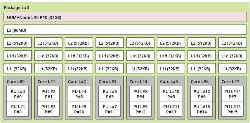
V-Cache prototype, shown at Computex last year, was indeed a 12-core dual-CCD chip, with fully functional 64 MB V-Cache on each 6-core (salvaged) CCD, for a full 192 MB total L3 cache. However, this was a prototype, which has not, so far, turned into full scale production. Limiting the demo to 12-core may have been down to package power and thermal limits, I guess, since 16-core is already constrained in the AM4 socket.