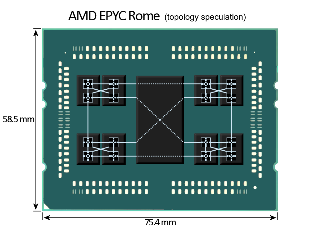
One issue is that, unless the Zen 2 cores are significantly taller and skinnier, there doesn't seem to be enough space on the die for two columns of 4 unless you kill the 32MB L3 cache rumour, or you stick a bunch of L3 on top of the columns in an asymmetric way. I was able to come up with this:
(snip)
Which just barely squeezes everything including 32MB of L3 inside the die, and that's with transistor scaling a bit on on the liberal side.
What scaling factor did you use for the cache? Note that SRAM shrinks down much more than logic when going 14LPP->7nm. According to wikichip, a high density SRAM bitcell is 0.027 µm² in TSMC 7nm and 0.064 µm² in Samsung/GloFo 14LPP, for a 0.42x shrink. The fact that SRAM scales so much better is basically why I think the caches got so big. It makes sense to spend more silicon on them when you get more in return.
I thought some here estimated about 270mm^2 for all the I/O stuff on the hub chip. If so, then 256MB of 14nm eDRAM L4 will be about 150mm^2 and WILL fit. My question is would AMD design it in a thick box partially depleted SOI process? They used to use such a process at 28nm. So they surely are familiar with thick box SOI. You would think IBM would restrict its use to themselves since the obvious application would compete with Power and the mainframe stuff. But then again IBM management is not known to think too far ahead. Plus Global has to maintain it and probably demanded it be included in the merger deal. But who knows? One question though. If no L4 eDRAM on the hub and no direct chiplet to chiplet connections, what can be so unique about this memory system that Papermaster advertizes as a generational improvement in overall latency to memory. I don't get it.
a) Directory with cache tags only -> still substantial amount of transistors due to 32*8MB of L3, but obviously saves a ton of area. For inter chiplet and inter chip, it is cache coherency agent
b) Directory with L4 cache -> the problem here is that L4 needs to be huge, 300+MB worth of transistors. Benefits are hard to quantify, as L4 needs to be huge to perform as cache, but in this case it is just keeping chiplet L3 content?
But with the L4 you would save 1 hop over IF to the chiplets L3 which means half the latency and also less power used. At the same time it saves bandwidth of the single chiplet-IO IF link meaning you can focus that link more on latency than bandwidth.
This of course depends how often you would actually need data in the cache of another chiplet. In a virtualized environment and cores assigned based on chiplets, you would never need data from another chiplet. However if you are doing heavy multi-threaded calculations, then certainly that will happen a lot. So it depends for what AMD wanted to optimize.
Even if you had an L4 thats fully inclusive on the I/O die that doesn't solve/ make memory requests between chiplets uniform. It infact makes the cache coherency protocol very complex. There will always be an extra cost going inter chiplet, its just were and how you pay for it(latency, power, total memory throughput).
But a fully inclusive L4 halves the latency.1 vs 2 IF hops. But yeah see above is it worth it? An non inclusive l4 per chiplet could actually make more sense as that would be useful in all scenarios. For me the problem with the inclusive L4 is that is will be 100% useless in virtualized environments as a chiplet running completely different VM will never need data from another chiplet. Unless I'm missing something here.
What scaling factor did you use for the cache? Note that SRAM shrinks down much more than logic when going 14LPP->7nm. According to wikichip, a high density SRAM bitcell is 0.027 µm² in TSMC 7nm and 0.064 µm² in Samsung/GloFo 14LPP, for a 0.42x shrink. The fact that SRAM scales so much better is basically why I think the caches got so big. It makes sense to spend more silicon on them when you get more in return.
I double checked and the scaling is right around 0.41-0.43x in that picture for L3 cache, which is a bit of a happy accident since I was unaware of the exact theoretical scaling, and somewhere in the range of 0.54-56x for the Zen cores, including L2.
Well, they could have fixed any number of issues with memory compatibility. I don't think we would have gotten a whole new front-end, but there were definitely problems worth addressing that wouldn't have cost a lot of silicon -- just time/iterations.
Here's an interesting quote, on a couple of levels
So, first, WRONG-Navas, no lower frequency AVX. :shrug: Ok, fine
But also, a hint about how far Rome really is away at this point "we don't anticipate" -- they don't know. I mean, this is probably *engineer* "know" but still. They don't know what quarter they're shipping, they don't know what frequency they're going to hit, they won't talk about IPC increase targets, and they won't commit to what they may or may not have to do about alleviating potential hot spots. Sounds to me like they have design targets, those design targets appear achievable, are well under way (controlled demos) and look to be less than a year away. But bad things can (and do) happen along the way. Does that sound right to you (all)?
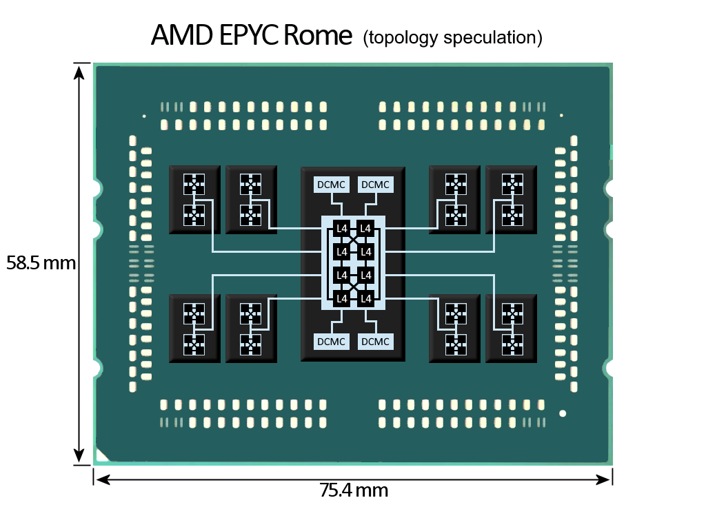
Here is my latest attempt to reconcile my ideas about a "quad-tree" topology with the latest information about Rome.
Mark Papermaster in his interview with AnandTech seems to have confirmed that there are no direct links between the CPU chiplets on the package — just a single IF link from each CPU chiplet to the IO chiplet. Also, many commentators have observed that the IO chiplet likely will include some kind of L4 for directory-based cache-coherence since snooping between CPU chiplets is expensive with a star topology.
It occurred to me that if the L4 is partitioned with one slice per CPU chiplet, and the partitions are grouped into fully connected quads, similar to the topology of the L3 in the quad-core CCX, we effectively have a "quad-tree" topology. However, unlike my previous attempt, in which I fully connected the CCXs in each pair of CPU chiplets into a cluster of 4 CCXs, the CCX cluster still consists of just two CCXs. AMD has instead reached 64 cores by expanding the top level of the hierarchy, effectively bringing two CPUs into one socket.
Thus, in my new attempt, the top and bottom partitions of the chip have a topology very much like Naples. While Naples had four 8-core chiplets fully connected by links on the package, Rome may have the four 8-core chiplets in each partition (top/bottom) fully connected via the L4 cache in the central IO chiplet.
If this topology is somewhat correct, AMD may not have reached full capacity in the socket yet! There is still room in this "quad-tree" topology to expand the CCX cluster to 4 fully connected 4-core CCXs (e.g. 16 cores per chiplet, or disintegrated into two 8-core chiplets). How will they fit that in the package? Well, they can put the IO and L4 in an active interposer, then mount each CCX cluster directly on top of its corresponding slice of L4 cache, hence achieve minimal L4 cache latency and more bandwidth through vertical links, while reducing the footprint.
Here is my latest attempt to reconcile my ideas about a "quad-tree" topology with the latest information about Rome.
Mark Papermaster in his interview with AnandTech seems to have confirmed that there are no direct links between the CPU chiplets on the package — just a single IF link from each CPU chiplet to the IO chiplet. Also, many commentators have observed that the IO chiplet likely will include some kind of L4 for directory-based cache-coherence since snooping between CPU chiplets is expensive with a star topology.
It occurred to me that if the L4 is partitioned with one slice per CPU chiplet, and the partitions are grouped into fully connected quads, similar to the topology of the L3 in the quad-core CCX, we effectively have a "quad-tree" topology. However, unlike my previous attempt, in which I fully connected the CCXs in each pair of CPU chiplets into a cluster of 4 CCXs, the CCX cluster still consists of just two CCXs. AMD has instead reached 64 cores by expanding the top level of the hierarchy, effectively bringing two CPUs into one socket.
Thus, in my new attempt, the top and bottom partitions of the chip have a topology very much like Naples. While Naples had four 8-core chiplets fully connected by links on the package, Rome may have the four 8-core chiplets in each partition (top/bottom) fully connected via the L4 cache in the central IO chip.
If this topology is somewhat correct, AMD may not have reached full capacity in the socket yet! There is still room in this "quad-tree" topology to expand the CCX cluster to 4 fully connected 4-core CCXs (e.g. 16 cores per chiplet, or disintegrated into two 8-core chiplets). How will they fit that into the socket? Well, they can put the IO and L4 in an active interposer, then mount each CCX cluster directly on top of its corresponding slice of L4 cache, hence achieve minimal L4 cache latency and more bandwidth through vertical links, while reducing the footprint.
Some of the earlier roadmaps had "Zen+" as a seperate step between Zen and Zen2 implying that the 14nm+ products would also receive architectural improvements but this was dropped pretty early on. Sadly, the Zen+ moniker stuck around and colored the perception of Pinnicle Ridge.
Some of the earlier roadmaps had "Zen+" as a seperate step between Zen and Zen2 implying that the 14nm+ products would also receive architectural improvements but this was dropped pretty early on. Sadly, the Zen+ moniker stuck around and colored the perception of Pinnicle Ridge.
In 2015 and 2016 AMD used "Zen+" as the next step after Zen. When Zen 2 was revealed in February 2017 "Zen+" wasn't used at all. Zen+ officially only reappeared in January 2018 when the 12nm Ryzen was announced to launch later in April.
By the way, here is a hypothetical Milan design, using the "quad-tree" topology on active interposer with embedded L4 (interposer illustrated in lighter green). With 8-core chiplets in a 4-by-4 grid, I am able to fit 128 cores in the package. Look closely, and you will see that the L4 structure on the interposer is the same as on the IO chiplet in my Rome diagram, albeit rotated 90 degrees. Without the top and bottom row of chiplets, you get the same topology as my Rome diagram, i.e. two CCXs per cluster. With the top and bottom row you get four CCXs per cluster and double the number of cores.
If you want to stick with 64 cores for Milan, you can also cut this design down the middle (and rotate it 90 degrees). That gives you four fully connected clusters (16 cores each) connected to four fully connected L4 slices, which seems more elegant (purer "quad-tree") than removing the top and bottom row.
PS. Although I have drawn each slice of L4 cache only covering part of one chiplet, this is arbitrary. You can make each L4 slice as big as you want it to be. Also, the diagram does not specify anything about how each CCX connects to the L4 (e.g. through an IF router, requiring an additional IF port in each CCX).
People who got this impression about 14nm+ stage being more than a simple refresh... did so by listening to AMD officials
When asked how long Zen would last, compared to Intel’s two-year tick-tock cadence, Papermaster confirmed the four-year lifespan and tapped the table in front of him: “We’re not going tick-tock,” he said. “Zen is going to be tock, tock, tock.”
Granted Zen+ was a good tick and Zen 2 looks like a tock of epic proportions, but the reality is this forum had tempered expectations about Zen+ due to it's own "collective wisdom", not based on whatever AMD promised.
Remember, with interposer you eliminate eight power-hungry IF links on package, so you'll have spare power to burn. Regarding hot spots, AMD has a paper on this by Eckert, Jayasena and Loh: "Thermal Feasibility of Die-Stacked Processing in Memory".
People who got this impression about 14nm+ stage being more than a simple refresh... did so by listening to AMD officials
Granted Zen+ was a good tick and Zen 2 looks like a tock of epic proportions, but the reality is this forum had tempered expectations about Zen+ due to it's own "collective wisdom", not based on whatever AMD promised.
But fair enough, it's possible that the consumer Zen+ tick originally wasn't planned. A lot of the improvements were "Ryzen done right" (PB2, PBO) and Ryzen 1xxx chips were the only Zen 1 ones affected by the 17 instead 12 (as spec) cycle cache access delay. But imo it's obviously nothing more than a refresh that was never going to get the man power and efforts Zen 1, 2, 3... are getting.
If we are assuming 2x 4-core CCX in each CCD (CPU Chiplet Die) then each quad (CCX) could be connected to a bus which would then be connected to a CCM (Cache-Coherent Master) which would be divided / partly duplicated (L3 tags etc.) between both sides of the IF-link from each CCD to the IOD.
The topology for the IOD could be a little better as currently there are 3 hops between some of the L4 cache slices. Intel has used many different topologies for their multi-socket servers, but in my opinion, this one looks the best for this kind of situation:
You can find the above diagram and more information here. Every processor is 2 hops away from any other processor. By connecting a pair of memory controllers where the IOHs sit, you get quite uniform access to them too. If you are using this topology for the IOD (between L4 slices) then why not use the same topology for the 8-core CCX (between L3 slices). Sure there will be some latency hits compared to fully connected one but this might be the best compromise for server workloads. It only requires 12 links compared to 6 links for fully connected quads. And still each L4 or L3 slice has direct access to 3 other slices.
That's my bet on 8C CCX and IOD topology but I could also be wrong. (Edit: More I think and read about, more likely it seems that there will only be 2x 4C CCXs in each chiplet. There's still some kind possibility of 8C CCX until otherwise proven and both designs have pros/cons.) What do you think? Also Vattila, if you could draw this topology, it would be much appreciated.
Addition: Each IOH (IO Hub) could have both two DD4 memory channels and 32x PCIe included in them or there could be different IO Hubs for DD4 pairs and groups of 32x PCIe. If memory controllers and Infinity Fabric run on different clocks then separate IO Hubs would quite likely be needed as an interface between different clock domains.
That is true. Granted. But the response was specifically against "Intel’s two-year tick-tock cadence". Epyc isn't on a two-year tick-tock cadence, it's apparently on a two-year tock cadence. I assumed a one year tock cadence. That's without talking about the timeframes that your quoted slide includes -- Zen3 coming well before 1Q2020 which I'm just going to place the likelihood of happening at this point at 0. Even generously, those Zen slabs align to about five quarters long each. If I were to take that slide at all seriously, I had to expect Zen2 by mid-2018. If it's a question between engineer's words, and marketing slides....
What would have been good to have gotten on the record (which as far as I know no one managed) was whether the low-hanging fruit was possible to pick up in a refresh, or whether the low-hanging fruit was specifically architectural in nature. That is...
It's obviously nothing more than a refresh that was never going to get the man power and efforts Zen 1, 2, 3... are getting.
...because I completely agree with your assessment here, the question was whether the low-hanging fruit was a matter of engineering or design. Because design wasn't going to happen until Zen2, while someone going in there and fixing memory compatibility, tweaking the IF to run at 2:1 to memory clock speeds (which was rumored to have existed, but been broken), and other stuff like that might well happen in a refresh. (To be fair, it appears that memory compatibility had some work done on it, but the progress wasn't stellar.)
If you prefer to argue from the slides, though, my basic question stands -- what happened to the 5-quarter tock schedule that's pictured in that slide? 7nm didn't land in 2Q2018. Did AMD think it was? [elide long, rambling, pointless guess as to what happened]
The interesting question to my mind is how much has changed due to the 7nm GF melt-down. AMD appears to have managed it quite well from the outside, but I expect there's a lot of duck paddling going on. Under something like the above scenario (which I just deleted -- sorry), Ryzen2 was meant to be slightly more than it was, TR2 is delivering a 32-core TR on the original (Epyc-like/lite) schedule, but without the benefits of process scaling or memory improvements, and Zen2 is likely to be more than it originally was. The most conservative guesses have already been proven wrong wrt chiplets, I expect the most conservative guesses regarding IPC are likely wrong as well. We'll probably know in two quarters, but guessing is fun.
It's not a new concept as you can find scientific articles referring to it at least as from 1991 (related to multi-cores). Still it's the best way of connecting 8 nodes with max 2 hops between each node without too much complexity. I'm sure there are many pros/cons with it but it's either something like this or some sort of ring bus.
Addition: Assuming 8C CCXs and/or IOD topology, the above might hold true. But it could also be quads (4 node crossbars) each connected with IF using bus topology. I really like the idea of this twisted cube topology though (edit: atleast for the IO die).
Cool. It looks like a possibility. As you point out, your topology has a lower diameter, so it may do better on big parallel workloads with interdependent threads across the whole CPU. At least, it may have better worst-case performance for threads running on cores far apart.
However, it doesn't do as well on locality and hence partitioning. A 4-core CCX with fully connected cores is a nice partition size. And on top level, my topology allows you to partition the CPU into two 32-core partitions, both of which have 4 fully connected CCX clusters.
With your topology, no subset with 4 cores or CCX clusters are fully connected. So your topology may do worse on workloads limited to a partition of the CPU — virtualisation, in particular.
You could always add 4 more links (to the twisted 3-cube topology) and have two fully connected quads and then have this twisted cube topology between the quads. That would be 16 links total. If you add two more links to the sides of your topology (from the topmost L4 slices to the bottom most slices) and twist the two middle ones, you would also get max 2 hops instead of 3. That's only 2 links more but their end points are quite far away, I'll give you that. Still something to think about.
That is true. Granted. But the response was specifically against "Intel’s two-year tick-tock cadence". Epyc isn't on a two-year tick-tock cadence, it's apparently on a two-year tock cadence. I assumed a one year tock cadence. That's without talking about the timeframes that your quoted slide includes -- Zen3 coming well before 1Q2020 which I'm just going to place the likelihood of happening at this point at 0. Even generously, those Zen slabs align to about five quarters long each. If I were to take that slide at all seriously, I had to expect Zen2 by mid-2018. If it's a question between engineer's words, and marketing slides....
What would have been good to have gotten on the record (which as far as I know no one managed) was whether the low-hanging fruit was possible to pick up in a refresh, or whether the low-hanging fruit was specifically architectural in nature. That is...
...because I completely agree with your assessment here, the question was whether the low-hanging fruit was a matter of engineering or design. Because design wasn't going to happen until Zen2, while someone going in there and fixing memory compatibility, tweaking the IF to run at 2:1 to memory clock speeds (which was rumored to have existed, but been broken), and other stuff like that might well happen in a refresh. (To be fair, it appears that memory compatibility had some work done on it, but the progress wasn't stellar.)
If you prefer to argue from the slides, though, my basic question stands -- what happened to the 5-quarter tock schedule that's pictured in that slide? 7nm didn't land in 2Q2018. Did AMD think it was? [elide long, rambling, pointless guess as to what happened]
The interesting question to my mind is how much has changed due to the 7nm GF melt-down. AMD appears to have managed it quite well from the outside, but I expect there's a lot of duck paddling going on. Under something like the above scenario (which I just deleted -- sorry), Ryzen2 was meant to be slightly more than it was, TR2 is delivering a 32-core TR on the original (Epyc-like/lite) schedule, but without the benefits of process scaling or memory improvements, and Zen2 is likely to be more than it originally was. The most conservative guesses have already been proven wrong wrt chiplets, I expect the most conservative guesses regarding IPC are likely wrong as well. We'll probably know in two quarters, but guessing is fun.
Others have mentioned it before, Zen+ was a filler because Zen 2 is taking longer. The slide I used only showing a vague timeframe imo already foreshadowed that while the roadmap is set the dates are moving targets still.
This is likely related to GloFo, but not only since even Vega 7nm, a straight port pipe cleaner, is taking longer than the optimistic regular timeframe. I personally think it's a combination of several development: GloFo opting out of 7nm. AMD approaching TSMC and likely also Samsung. 7nm in general taking longer. Intel still being unable to deliver their next or even any new node, meaning the time pressure by the market is not there yet. AMD's approach is clearly ambitious, to me it seems they currently allow themselves more time than originally planned to do it right.
As for what would have been possible with Zen+, my impression is that all its improvements are due to tighter testing and updated microcode as well as the updated node, not changes in the silicon. So Zen+ improvements were mostly the low-hanging fruits above the silicon level (most of which were developed as part of Raven Ridge), whereas with Zen 2 the whole silicon design and overall system architecture can be revised for further low-hanging fruits.
Interesting thoughts. Cant wait to see epyc in action.
Man as AMD said they are only starting.
If i am wrong please corrent me... for years we were watching 1-5% intel pushig their cpu every 2 years. Basically they were improvinf ipc, bur loosing frequency... after skylake they are improvinf only frequency. AMD improved 3% ipc and ~8% speed (+10% mem latency was decreased) in a year. Still not two years...
One question though. If no L4 eDRAM on the hub and no direct chiplet to chiplet connections, what can be so unique about this memory system that Papermaster advertizes as a generational improvement in overall latency to memory. I don't get it.
I do get how this improves on worst-case socket-to-socket latency greatly in 2S systems but I don't get either how this would without questions be a better topology than what Naples currently has. I get the manufacturing benefits very well, though. If we assume that chiplet to IO die IF-links in Rome have about the same latency as IFOP links in Naples then additional improvements (eDRAM buffer/L4, prefetching, etc) are absolutely required and may not even be enough. If we're are not counting NUMA then Naples already has perfectly usable latencies: https://www.anandtech.com/show/11544/intel-skylake-ep-vs-amd-epyc-7000-cpu-battle-of-the-decade/13
AMD's slides show that local memory access round trip takes about 90ns:
On-package latency to other Zeppelin's memory controller with one additional IFOP hop and through other SDF is about 145ns which is 55ns more than access to local memory. Then replacing IFOP hop with socket-to-socket IFIS hop (200ns) adds another 55ns to the previous case and 110ns to local access. Then there's the worst case situation crossing first one IFIS and then one IFOP on the second processor which may have latency of about 255ns. So it's not hard to see that 2S worst-case latencies can be easily improved over Naples.
In summary, if I have interpreted everything correctly, Naples have the following latencies:
Local memory access ~90ns
Additional IFOP (Infinity Fabric On-Package) hop during memory access ~55ns
Additional IFIS (Infinity Fabric InterSocket) hop during memory access ~110ns
And the total latencies should be:
Local memory access ~90ns
IFOP hop + memory access ~145ns
IFIS hop + memory access ~200ns
IFIS hop + IFOP hop + memory access ~255ns (?) (presented here)
Local cross-CCX latency (tested here) should be a little lower than IFOP hop + memory access or about ~111ns to ~140ns depending on memory speeds
If we would just assume that chiplet to IO die latency would be about the same as single IFOP hop (~55ns) and IO die to memory latency would be about the same ~90ns then the best case memory latency for EPYC Rome would be ~145ns which is not good. In order for this to work AMD has to have improved both memory latency and especially IFOP 2.0 latency greatly. The weakest point of this design would be if the IFOP 2.0 latency would be too high. They can obviously keep copies of the L3 cache tags on IO die but still, there are many possible weak points. Adding maximum amount of L3 cache to each chiplet would obviously help and so would large enough L4 cache.
Sorry for oversimplifying this to myself but I'm still mostly as confused about this design as I was about a week ago. I guess we have to still wait for more information but 2x 4C CCX vs. 8C CCX is not the biggest deciding factor here, chiplet to IO die latency is. I'm sure that AMD have thought this well through and the memory system is just fine.
2.35GHz 64c unknown rome vs highest freq 32 core 7601 that tops out at at 2.2GHz.
We need to know tdp but they hardly cant push 4 times as much fp at same tdp.
This site uses cookies to help personalise content, tailor your experience and to keep you logged in if you register.
By continuing to use this site, you are consenting to our use of cookies.


.png")