64 core EPYC Rome (Zen2)Architecture Overview?

Page 24 - Seeking answers? Join the AnandTech community: where nearly half-a-million members share solutions and discuss the latest tech.

H T C

Senior member
Nov 7, 2018
549
395
136
For me, the really big question is whether AMD has the packaging capacity and low cost to take chiplet design into the mainstream. If so, then we'll see reuse of their 7nm CPU chiplet for the Ryzen 3000 series. They only need a mini IO chiplet.

What is the easiest way for AMD to create this IO chiplet? They already have Raven Ridge. It has the dual-channel memory controllers and IO needed. Just rip out the 4-core CCX and replace it with some external IF ports to connect the CPU chiplet. Except for that, and some adjustment to the layout, no redesign is needed. With this seemingly simple solution, Ryzen 3000 would come with a powerful iGPU as well, thus match Intel's feature set and increase sales with OEMs.

Drivers for this thing would be mostly based on Raven Ridge and ready to go.

Would it fit on the package? 14LP Raven Ridge sans CCX is 166 mm² (210 - 44). With the announced 15% density improvement for 12LP we get 144 mm², so let's say 150 mm² for good measure.

9114301_c454443b5feb4f8465a65f148c87a626.png

Stupid question: what if AMD just shrink's Vega 56 to 7nm but change it enough have IF, just like the latest Instinct family cards, and have that placed on the CPU, HBM2 included?

The idea was to have a CPU chiplet + an IO chiplet + Vega-like 7nm full chip and have the whole thing work as an APU.

Is it @ all possible?

EDIT

Due to power constraints, it would most likely require quite a slimmed down version of Vega 7nm chip, but still a full chip: thinking along the lines of a RX460 Polaris level of performance perhaps, but on a Vega design.
 
Last edited:

Gideon

Golden Member
Nov 27, 2007
1,619
3,645
136
The thing to note is that the previous generation for Intel (Core 2 Duo) still had FSB and a memory controller in its chipset. You have to remember that context. So this memory controller in a separate die thing might have been an improvement back then, but if Intel was coming from a platform that had a memory controller on-die at that time, it would likely have been a regression performance-wise. And very likely also for power consumption in a mobile platform. The memory interface is very busy and anything that crosses substrate usually eats power. Not a good combo.

I have never claimed that moving the memory controller off-die is somehow an improvement to latencies. The only thing I'm trying to get through is, that:

Despite the on-die memory controller, latency in Zen is so terrible that even if Zen 2 goes with chiplets, it has some room for improvement.

The slowness of the current architecture is probably due to 1st gen Infinity Fabric running at memory speed, even on-chip. There is no inherent reason why it must be as terrible on Zen 2. Zen 1 has worse latency than all recent AMD designs (Bulldozer, Phenom, A64). It's also even worse than on chips with memory controllers off-die, like Core 2 and some Nehalem variants.

The aforementioned Nehalem chip (Clarkdale) was actually released after Lynnfield (which already had the memory controller on-die) and sure enough the latencies are nearly 2x worse.

BTW:
Cat_merc just linked to a very interesting interview with AMD's Daniel Bounds discussing EPYC 2, which also touches the subject a bit.

Among other things he mentiones, that the chiplets are actually called CCD's (Core Complex Die?). Also that they'll release more info about latencies and stuff in Q1 or Q2.
 

Arzachel

Senior member
Apr 7, 2011
903
76
91
If they include an iGPU at all, I would be surprised to see one smaller than the one in Raven Ridge (11 CU). Below that, they'll quickly run into diminishing returns. Polaris 11 (16 CUs) is a 123mm^2 chip; Polaris 12 (8 CUs) is a 103mm^2 chip. That's a lot of lost functionality for not much saved space. No matter how few CUs, they still need the video output hardware and encoding/decoding fixed-function hardware. Of course there's also some stuff that can be omitted on an iGPU because it's shared with the CPU, most notably the memory controller.

Dedicated GPUs aren't a good comparison, since those are likely pad limited. Looking at the Raven Ridge die shot, I'd guess at 40-50mm2 for just the CUs.

I'm kind of torn on this because you'd think that the iGPU would benefit from a die shrink, but having more than ~12CUs seems like a massive waste unless you have the memory to feed them so I'm kinda coming around to the idea of integrating the GPU cores into the IO die, for the low end at least. Still hoping for a Navi chiplet hooked up to 1Hi HBM2 through IF.
 
  • Like
Reactions: amd6502

Tuna-Fish

Golden Member
Mar 4, 2011
1,346
1,525
136
If each chiplet has a local 32MB L3 cache, is L4 cache (on I/O die) smaller than 256MB (128MM or 64MB) even beneficial or needed? Does it improve memory lantecy by how much? Does it reduce cache misses by a significant amount?

The primary reason you want a cache there is that to maintain cache coherency, you absolutely want the IO die to know exactly where each line in cache loaded from the attached memory channels currently resides. If the IO die doesn't know that, on every memory access the system has to query every cache in the system. This is how cache coherency worked in the era of dual cores, but that starts being painful when you move up to quads and at >8 cores, you can just forget about it.

So you attach a directory structure that contains occupancy information for every line in the system. The thing is, that structure is basically identical to cache tags. Querying it costs the same amount of latency as querying a cache for occupancy. So when you have that, you might as well expand it a bit, and add actual storage, turning it into a real L4 cache.

The big question in my mind is not if there is a cache. It's not even whether the all the lines all the caches of the chiplets must also allocate a tag from the L4, I would be extremely surprised if they didn't. The question is whether the all the data in the lower levels is required to be fully replicated in the L4. That would be possible with eDRAM.

Note that I fully expect the L4 to be memory-sided, and split per controller. That is, each memory controller (in past AMD designs, each controller has two channels, so 4 controllers per EPYC IO die) actually has it's own separate L4 cache and only lines from that memory controller can reside there. This substantially reduces the latency hit of looking at the L4 tags.
If not actually split per controller, then at least split into two halves, for top/north memory controllers and down/south controllers.


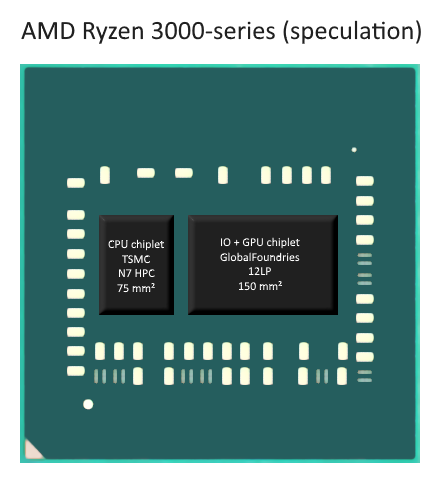
If each chiplet would contain just two 4-core CCXs, why didn't AMD use four 146 mm² chiplets with four 4-core CCXs instead what they have done now (eight 73 mm² chiplets)? Do chiplets have to be 8-core CCXs for current design for Rome to make any sense? AMD didn't choose 8-core chiplets just because of yields or binning for higher clocks / better power efficiency. They must have had some architectural reasons behind it, right? 7 nm Vega is a relatively big chip so 146 mm² chiplet would have been ok.

Yes. All else being equal, if your product fits into a smaller die, smaller dies are better all the way down to ~20mm^2 or so. There are always some errors that lead to chips that are unharvestable even at lower core counts (like shorts between power and ground), so the smaller your die, the less you lose. Also, smaller dies lead to less loss caused by the edges of wafer. I think the idea of putting two CCX on a single chiplet is not something anyone ever proposed -- it's just cost without benefit once all communication needs to go through an external chip anyway.

Once they decided to go with chiplets, design tradeoff they optimized was the size of CCX vs size of die. Larger CCX are better because single-threaded performance still matters, and the bigger the CCX the more L3 cache a single thread can make use of. Denser future fabrication processes will almost certainly lead to even smaller chiplets.
 

Abwx

Lifer
Apr 2, 2011
10,937
3,440
136
I think it would be plenty worthy differentiation if 7nm Zen 2 beats 14nm Skylake/CFL as I expect it to — and at lower power to boot. If AMD fails me and does not, it may make more sense to fight the high end with Threadripper 3000. If it has UMA and L4 cache as presumed, it may even perform better on games and other latency-sensitive applications than Ryzen 3000.

An AMD representative said that Zen 2 was designed to compete favourably with 10nm ICLake and that they anticipated Intel as being very agressive perf wise for this gen.

This mean that they had to take account of an eventual 10% improvement in IPC as well as 10% frequency uplift, but also of the possible core count increased from 56C to 64C (+14.28%) and Intel being even in this register.

To keep being competitive they had to target at least 21% better perf/core frequency and IPC combined.

....we planned against a very aggressive Intel roadmap, and I really Rome and Milan and what is after them against what we thought Intel could do.

Rome was designed to compete favorably with “Ice Lake” Xeons

https://www.nextplatform.com/2018/06/20/amds-epyc-return-to-the-datacenter-ring/
 

amd6502

Senior member
Apr 21, 2017
971
360
136
JDG1980 said:
If they include an iGPU at all, I would be surprised to see one smaller than the one in Raven Ridge (11 CU). Below that, they'll quickly run into diminishing returns. Polaris 11 (16 CUs) is a 123mm^2 chip; Polaris 12 (8 CUs) is a 103mm^2 chip. That's a lot of lost functionality for not much saved space. No matter how few CUs, they still need the video output hardware and encoding/decoding fixed-function hardware. Of course there's also some stuff that can be omitted on an iGPU because it's shared with the CPU, most notably the memory controller.

Dedicated GPUs aren't a good comparison, since those are likely pad limited. Looking at the Raven Ridge die shot, I'd guess at 40-50mm2 for just the CUs.

I'm kind of torn on this because you'd think that the iGPU would benefit from a die shrink, but having more than ~12CUs seems like a massive waste unless you have the memory to feed them so I'm kinda coming around to the idea of integrating the GPU cores into the IO die, for the low end at least. Still hoping for a Navi chiplet hooked up to 1Hi HBM2 through IF.


Good point about P12 quite possibly being pad limited as it's running into minimum die size.


I also guestimate a CU of about 5mm2 in 14nm Vegas.

The GPU uncore in P12 and P11/P21/rx560 I guess is 35 ~ 40mm2, with a good portion of it being memory controller+interface, the rest display engine. Therefore in RR we don't count the memory controller+interface as GPU uncore (since we consider it CPU uncore) and it's going to be just ~ 20mm2 for the graphics overhead.

That's a very small overhead for a huge selling point; it is a really nice thing to have temporary/fallback or backup on desktop, and it's almost a must-have for mobile parts. From then on it's ~40mm2 for every 8 CU's of Vega. So 60mm2 should get you an 8 CU iGPU.

With the 40mm2 per 8 CU guestimate it pegs RR's 11CU as 55mm2 and RR's GPU portion of the die at ~75mm2.

They could just spend the 55mm2 on an identical CU count as RR, or skimp with a Vega 3 (15mm2) and knock off a whole 40mm2 which is substantial in my opinion.

11CU is really a bit overkill for mobile optimized CU count, and a large number of RR are harvested with just 8CU enabled. Laptops often run on dual channel 2133, and so even 6CU@1ghz would do (though 8CU is more optimal for perf/watt) to almost max out the GPU. Something in between 3 and 11 maybe; 6CU at 30mm, making the GPU portion 50mm2 and the IF+memory interface portion and uncore another 50mm2, with total die sieze then at 100mm2 which probably is very close to the minimum die size for all the IO and inf fabric connections. I think 6-8CU is the sweet spot with everything considered.

On an unrelated topic, does anyone know if chiplets can be tested and crudely binned before being used in MCM, other than by having computers look at it with microscopes?
 
Last edited:
  • Like
Reactions: Vattila

Vattila

Senior member
Oct 22, 2004
799
1,351
136
The idea was to have a CPU chiplet + an IO chiplet + Vega-like 7nm full chip and have the whole thing work as an APU.

Aye — I'm sure AMD's high-performance APU with HBM will arrive at some point. It is what I have termed AMD's "super APU" in my speculation thread on this matter (here).

I think the idea of putting two CCX on a single chiplet is not something anyone ever proposed -- it's just cost without benefit once all communication needs to go through an external chip anyway.

Hold on — you are assuming a CCX is 8 cores with some new topology. This has not been confirmed yet, as far as I know. AMD fellow and researcher, Gabriel Loh, pretty consistently draws cores in 4-core direct-connected complexes in his research papers on topology. Even in his paper on concentrated mesh topologies, each node in the mesh routes to a 4-core complex. So, until I see confirmation that the 4-core CCX has been abandoned, I'll stick to that.

An AMD representative said that Zen 2 was designed to compete favourably with 10nm Ice Lake and that they anticipated Intel as being very aggressive performance-wise for this gen. This mean that they had to take account of an eventual 10% improvement in IPC as well as 10% frequency uplift, but also of the possible core count increased from 56C to 64C (+14.28%) and Intel being even in this register. To keep being competitive they had to target at least 21% better perf/core frequency and IPC combined.

Yeah. Several AMD executives have stated this. Lisa Su must have seen a way to compete with 10nm Ice Lake by now, when she decided to take AMD back to fighting Intel in high-end compute. Targetting anything less for Zen 2 would have been a folly.

I think it would be hard to be disappointed that AMD is targeting the server market with higher core counts while still recognizing the importance of more performant, lower core-count parts.

It is not that I am disappointed with AMD. I am full of admiration for what Lisa Su has achieved so far, as she has lead the company from deathbed to sustained profits.

But I set my expectations based on what I see would be a reasonable business plan. Planning to lose against 14nm Skylake/CFL at a time when 10nm Ice Lake was expected to be in the market, with Ice Lake having architectural improvements, increased density (core count), lower power and higher performance — as originally projected for Intel's 10nm process — that is not a sound business plan.

If 10nm Ice Lake was here by now, with performance as originally envisioned, I would have accepted that Zen 2 might have had slight losses in some areas, provided it could reasonably compete in profitable areas, and with the promise of Zen 3 around the corner. As Lisa Su likes to remind us, their roadmap is solid, but it is "a journey" which requires patience and steadfast execution.

However, Ice Lake is not here. AMD has an unprecedented opportunity. Intel is having big problems with their roadmap. 7nm Zen 2 is now facing 14nm Skylake-derivatives, and we should expect it to win decisively — unless AMD has fallen short of targets.
 
Last edited:

Vattila

Senior member
Oct 22, 2004
799
1,351
136
On an unrelated topic, does anyone know if chiplets can be tested and crudely binned before being used in MCM, other than by having computers look at it with microscopes?

I am not an expert, but this is called Known Good Die (KGD) and is widely deployed in die testing and MCM packaging to increase fully assembled package yield. Otherwise you quickly get very high probability of failure as the number of chips increase (the probability that the package is good is the product of the probabilities of each component being good, so falls pretty quickly with increasing number of components).
 
  • Like
Reactions: amd6502

Vattila

Senior member
Oct 22, 2004
799
1,351
136
does anyone know if chiplets can be […] binned before being used in MCM

I presume they do. Binning, i.e. sorting the chiplets by performance, is a big benefit of chiplet design. You can increase the performance of the assembled package substantially by using chiplets from the top bins. AMD research describes ~30% improvement of the top bin for a 64-core chip with quad-core chiplets versus a monolithic design (~23% improvement in the peak bin). With 8-core chiplets, "Rome" probably sees a little less benefit.

See this video by AdoredTV: https://youtu.be/G3kGSbWFig4?t=596
 
  • Like
Reactions: amd6502

maddie

Diamond Member
Jul 18, 2010
4,738
4,667
136
On an unrelated topic, does anyone know if chiplets can be tested and crudely binned before being used in MCM, other than by having computers look at it with microscopes?

I presume they do. Binning, i.e. sorting the chiplets by performance, is a big benefit of chiplet design. You can increase the performance of the assembled package substantially by using chiplets from the top bins. AMD research describes ~30% improvement of the top bin for a 64-core chip with quad-core chiplets versus a monolithic design (~23% improvement in the peak bin). With 8-core chiplets, "Rome" probably sees a little less benefit.

See this video by AdoredTV: https://youtu.be/G3kGSbWFig4?t=596
I consider this one of the great unsung benefits of chiplets. Very unlikely to have a 64 core die monolithic die with all cores close to equal. Bin for speed, power, etc.

Here's the paper, check pg 2: http://www.eecg.toronto.edu/~enright/Kannan_MICRO48.pdf
 

IRobot23

Senior member
Jul 3, 2017
601
183
76
I want to know latencies of this design, I cannot see how can this be better for gaming than older "R7 2700X" if it will have same design.
 

DrMrLordX

Lifer
Apr 27, 2000
21,617
10,826
136
I believe Charlie said EPYC2 release in 19Q2 and Ryzen3 in 19Q3/4?

That seems wrong. AMD has already said Q1 2019 for Rome and Q2 2019 for Matisse. AMD would be missing out majorly if they delayed any further than now. Now is the time to strike.

Some people here mentioned that Intel Clarkdale (2010 Nehalem Arch) also has a separated Northbridge on package. Thanks for pointing that out, I had totally forgotten about the CPU.

The overall layout of Clarkdale is actually a bit similar to the one Vattila described above (with the GPU being on the NB). Though not excatly as the CPU still does some of the (legacy) I/O:

The latency on i5 661 is indeed nearly 2x worse than with the on-die controller i5's. Curiously the i5 661 did even worse than the Core 2 Q6600

And yet even the i5-661 has lower memory latency than a 2700x.

I want to know latencies of this design, I cannot see how can this be better for gaming than older "R7 2700X" if it will have same design.

Zen/Zen+ has to go through an IF link to get to a memory controller no matter what, even if the memory controller is on the same die. The speed of your IF link affects memory latency. If you move your memory controller off-die, connect it to the chiplet via IF, and speed up your IF link considerably (and make it wider), you can have better latency between the requesting core and the target memory controller. That, in turn, could reduce memory latency.
 

IRobot23

Senior member
Jul 3, 2017
601
183
76
That seems wrong. AMD has already said Q1 2019 for Rome and Q2 2019 for Matisse. AMD would be missing out majorly if they delayed any further than now. Now is the time to strike.


And yet even the i5-661 has lower memory latency than a 2700x.


Zen/Zen+ has to go through an IF link to get to a memory controller no matter what, even if the memory controller is on the same die. The speed of your IF link affects memory latency. If you move your memory controller off-die, connect it to the chiplet via IF, and speed up your IF link considerably (and make it wider), you can have better latency between the requesting core and the target memory controller. That, in turn, could reduce memory latency.

Okay,
would be worth making 100-130mm^2 die size + 73mm^2 against ~ 160mm^2
 

itsmydamnation

Platinum Member
Feb 6, 2011
2,764
3,131
136
Okay,
would be worth making 100-130mm^2 die size + 73mm^2 against ~ 160mm^2
yes,
think about it from a total potential revenue perspective, 7nm capacity will be the limiting factor.
Also if amd want to do >8 cores on AM4 then it really starts to pay because they can do single or dual chiplets and there is no wasted 7nm silicon.


edit: if i was amd i would do upto 12cores for amd 4 this time as max for am4 and then to 16 with the 7nm+ / hopefully DDR5.
 

PotatoWithEarsOnSide

Senior member
Feb 23, 2017
664
701
106
I'm not sure that we will see dual chiplets on AM4.
Unless yields are through the roof, and capacity is also increased significantly, I don't see how AMD could even meet demand if performance is at the levels that we're hoping for. For dual chiplets to work financially, the premium on the 16C CPU would have to justify them not being sold as separate 8C CPUs.
Everything below 8C would likely use a defective die, so I consider them to be free yield.
So it comes down to whether a) there is a demand for 16C AM4, and b) whether the margins on a 16C CPU was greater than on 2x 8C CPUs.
The demand would likely be lower than TR, since it has more memory channels to feed the extra cores, so the cost would also likely be limited by TR pricing.
That being said, DDR5 and 16C AM4 might have demand, though that would be Zen 3 anyway.
 
  • Like
Reactions: beginner99

Gideon

Golden Member
Nov 27, 2007
1,619
3,645
136
That seems wrong. AMD has already said Q1 2019 for Rome and Q2 2019 for Matisse. AMD would be missing out majorly if they delayed any further than now. Now is the time to strike.
I really hope I'm wrong, but Q2 for Rome might not be that might not be that far off from the truth. Even in the Daniel Bounds interview he said that they'll tell us more about the interconnect in Q1 or Q2. There wouldn't be any reason to keep any info secret, once the product is already on the market.
Hopefully, if Rome takes longer, they still release Ryzen on time.
 

itsmydamnation

Platinum Member
Feb 6, 2011
2,764
3,131
136
I'm not sure that we will see dual chiplets on AM4.
Unless yields are through the roof, and capacity is also increased significantly, I don't see how AMD could even meet demand if performance is at the levels that we're hoping for. For dual chiplets to work financially, the premium on the 16C CPU would have to justify them not being sold as separate 8C CPUs.
Everything below 8C would likely use a defective die, so I consider them to be free yield.
So it comes down to whether a) there is a demand for 16C AM4, and b) whether the margins on a 16C CPU was greater than on 2x 8C CPUs.
The demand would likely be lower than TR, since it has more memory channels to feed the extra cores, so the cost would also likely be limited by TR pricing.
That being said, DDR5 and 16C AM4 might have demand, though that would be Zen 3 anyway.

There is also halo, king of performance to consider, intel will max out the core clocks, the uncore clocks, push the TDP's on an 8 core 14nm refresh. a 12 core AM4 part means there is nothing intel can do, AM4 at 8 core only means intel will probably just pip amd on cpu performance ( yes at very high power) just from raw clock speed.
 

Spartak

Senior member
Jul 4, 2015
353
266
136
That seems wrong. AMD has already said Q1 2019 for Rome and Q2 2019 for Matisse. AMD would be missing out majorly if they delayed any further than now. Now is the time to strike.

When did they ever state that? Also, schedules change. Charlie has indeed stated Q2 for Rome. In a tweet I can't find right now he stated Matisse for Q3/4, straight from the source.

I have to say I believe this rumored timefrime to be true. People thinking Rome in Q1, Matisse in Q2 will be in for a major disappointment.

Rome 19Q2:
https://www.semiaccurate.com/2018/11/09/amds-rome-is-indeed-a-monster/
 
Last edited:

DisEnchantment

Golden Member
Mar 3, 2017
1,601
5,780
136
My thinking is that the 16 core parts are best served by the TR series. The AM4 will continue to deliver great value under USD 300. I imagine users going for 16 cores are the kind that would want more PCIe lanes and extra memory channels etc which is basically TR territory.
Above it starting from 8 to 32 Cores will be the Quad Channel Memory using Threadripper 3. AMD would be interested to entice such users in to their TR4 platform.

The 'Castle Peak'
uDJITku.jpg


Those new platform features could likely be PCIe 4.0, new chipset and lots of NVME slots.

Also Daniel Bounds reiterated that there will be no separate NUMA domains for Rome and therefore TR3.

Next year I am going Threadripper, Interesting times.
I am drooling at the prospect of 32 Core TR3, with quad 3600+ MT/s Memory channels which is good at everything and lots of IO. It would be a great product even at 4.0 GHz.
 

PotatoWithEarsOnSide

Senior member
Feb 23, 2017
664
701
106
As much as the halo argument makes sense, we know that Intel won't get away with another 9900k-esque product with the reviewers. If AMD can compete/beat with/the 9900k in unlimited mode, then AMD really doesn't need more cores on AM4.
The 9900k launch debacle has lost many hearts and minds, despite the fact it is a phenomenal product. There's a clear momentum swing in the market at the moment, and if Zen 2 does hit the spot then I think Intel are in a tricky spot for a good few years. For me, the next inflection point will be the respective performance of Intel/AMD when DDR5 hits the market.
 

IRobot23

Senior member
Jul 3, 2017
601
183
76
yes,
think about it from a total potential revenue perspective, 7nm capacity will be the limiting factor.
Also if amd want to do >8 cores on AM4 then it really starts to pay because they can do single or dual chiplets and there is no wasted 7nm silicon.


edit: if i was amd i would do upto 12cores for amd 4 this time as max for am4 and then to 16 with the 7nm+ / hopefully DDR5.

Don't dream about it. 16C way to high for AM4. Actually there is not much space for dual chiplets 7nm+ 14nm chiplet at all.. then power deliver/pins and so on. You have to understand that ZEN2 is way larger than ZEN/ZEN+. There is also support for 512bit AVX which will be competitive with intel.

Power deliver per per pin might be problem for 16C. If they are going for low latency then even SOC might use like 15-30W.

Imagine that single CCX on RYZEN 1000 takes around 44mm^2 while whole package of 8 cores on 7nm RYzen (3000*) will take ~73mm^2.

7nm should be like 60% die of 14nm.
Ryzen should be like 88-90mm^2 (2x CCX) - lets take 95mm^2 for whole package ~= 57mm^2 for ryzen 1000 and 2000 (zen/+). Assuming that L3 stays same then they had do increase at least 2mm^2 per core (L1+L2).

If they decide for 16C on AM4 then they will have to loose in latency which is actually one thing that is not comparable with intel. How well would ryzen do with 40-45ns DRAM latency? Or how bad would intel do with 60-70ns latency?
 

DisEnchantment

Golden Member
Mar 3, 2017
1,601
5,780
136
As much as the halo argument makes sense, we know that Intel won't get away with another 9900k-esque product with the reviewers. If AMD can compete/beat with/the 9900k in unlimited mode, then AMD really doesn't need more cores on AM4.
The 9900k launch debacle has lost many hearts and minds, despite the fact it is a phenomenal product. There's a clear momentum swing in the market at the moment, and if Zen 2 does hit the spot then I think Intel are in a tricky spot for a good few years. For me, the next inflection point will be the respective performance of Intel/AMD when DDR5 hits the market.

DDR5 likely late 2020/early 2021.

In the sales roadmap below it is not specified which core will be used for Vermeer
f7VraeV.jpg


However according to this roadmap below, there is a chance Vermeer could go with Zen3. Also fits Papermaster's `tock`, `tock`, `tock` roadmap :D
Vermeer Core has not been specified. And the process optimization has not been specified.
If Vermeer is Zen3 + TSMC's 7nm+ then the outlook is fairly good for desktop users.
Gamers Nexus reported mid of this year that AMD is working with DDR5 from like 5 months ago.


iYVoMUR.png


eN8j7Jv.png
 
Last edited:

Spartak

Senior member
Jul 4, 2015
353
266
136
My thinking is that the 16 core parts are best served by the TR series. The AM4 will continue to deliver great value under USD 300. I imagine users going for 16 cores are the kind that would want more PCIe lanes and extra memory channels etc which is basically TR territory.

This is actually why I don't understand the choice for an 8CCX. A 6CCX could have a similar dual setup as the current desktop CPU's and would enable 12C/24T for the desktop. 6-12C for desktop and 4-6C for mobile to me seems the sweet spot for consumers-enthusiasts the coming years.

But maybe (much) higher IPC plus high clocks eats so much TDP and delivers so much extra performance, AMD is secure enough they can win the desktop with 8 cores.

There is also the remote posibility that the 8CCX Rome chiplet will differ from the CCX for desktop and mobile. If you already design an entirely different SOC why not have the CCX arrangement be different as well? It might also explain why Matisse is expected for Q3/4.
 
Last edited:

exquisitechar

Senior member
Apr 18, 2017
657
871
136
When did they ever state that? Also, schedules change. Charlie has indeed stated Q2 for Rome. In a tweet I can't find right now he stated Matisse for Q3/4, straight from the source.

I have to say I believe this rumored timefrime to be true. People thinking Rome in Q1, Matisse in Q2 will be in for a major disappointment.

Rome 19Q2:
https://www.semiaccurate.com/2018/11/09/amds-rome-is-indeed-a-monster/
Correct. He even said that it's likely Q4 rather than Q3 for Matisse, sadly.
 

itsmydamnation

Platinum Member
Feb 6, 2011
2,764
3,131
136
Don't dream about it. 16C way to high for AM4. Actually there is not much space for dual chiplets 7nm+ 14nm chiplet at all..
You realise we are taking 200-250mm sq for two chiplets + IO with 2x DDR, 32pci-e + sata usb etc?. Thats prefectly fine for AM4.

then power deliver/pins and so on.
Explain Rome then

You have to understand that ZEN2 is way larger than ZEN/ZEN+. There is also support for 512bit AVX which will be competitive with intel.
NO AVX512 support, i dont even think AMD has cross license for it. Zen2 gets 256bit wide L/S, FRPF and FPU SIMDS. It wont add that much space given that 8cores + cache and IF are fitting in 70mm sq. For an example look at skylake vs skylake X core ( minus the home agent for X).

Power deliver per per pin might be problem for 16C. If they are going for low latency then even SOC might use like 15-30W.
This isn't anything new dont you remember AM3?


Imagine that single CCX on RYZEN 1000 takes around 44mm^2 while whole package of 8 cores on 7nm RYzen (3000*) will take ~73mm^2.
Whats your actual point? But just to argue the point, if it has double the L3 cache like rumored then thats about 4 cores worth of die size by itself and it still needs the I/O + other bits ( where does memory decrytpion happen for example). 1/2 a chiplet could be L3 cache, that would make each Zen 2 core about 4-5mm sq incl L2.


7nm should be like 60% die of 14nm.
Ryzen should be like 88-90mm^2 (2x CCX) - lets take 95mm^2 for whole package ~= 57mm^2 for ryzen 1000 and 2000 (zen/+). Assuming that L3 stays same then they had do increase at least 2mm^2 per core (L1+L2).
If we are just going to make up numbers i could easily do the same to support my position.


If they decide for 16C on AM4 then they will have to loose in latency which is actually one thing that is not comparable with intel. How well would ryzen do with 40-45ns DRAM latency? Or how bad would intel do with 60-70ns latency?
So you have no idea how cache cohernecy/memory accesses work on the new chiplet+I/O die. Second we already have an idea, for most workloads sweet FA. For gaming its very quickly hits minimal returns ( see the stilts mem clock + low latency timings benchmark data).