64 core EPYC Rome (Zen2)Architecture Overview?

Page 20 - Seeking answers? Join the AnandTech community: where nearly half-a-million members share solutions and discuss the latest tech.

Vattila

Senior member
Oct 22, 2004
799
1,351
136
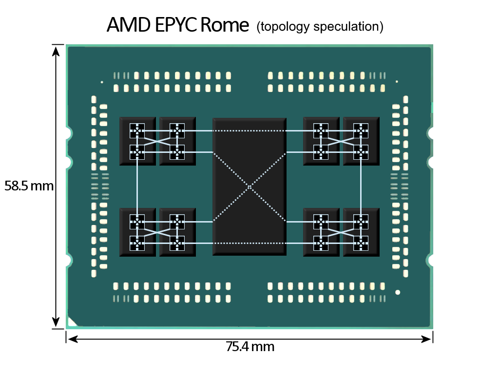
AMD sure likes to use crossbar topology wherever they can and see fit.

Yeah. Fully connected quads on every hierarchical level, from cores to dies, seems to have been the thinking with the Zen system architecture — except that on two levels, CCXs and sockets, there were only pairs in Naples. I have speculated that the obvious way to evolve the architecture would be to fill out these levels to quads, i.e. 4 fully connected CCXs, and 4 fully connected sockets. That would bring the system core count to 256 cores.

With Rome, it seems to me they have done just that, albeit in a surprising way by disaggregating the CCX cluster into two chiplets. This makes sense for die yield and binning, as well as reuse across market segments. With my interpretation, nothing much has changed as far as core topology is concerned. Rome simply extends the number of CCXs in a cluster from two to four over two chiplets.

And regarding 4 fully connected sockets, could a new socket/interconnect for 4S systems be the mysterious "ZenX" rumour that AdoredTV was reporting? The "quad-tree" topology sure spells out "X" on every level.

9114301_e1a94b72c27cb164aa4fbd4656b4bbf8.png
 
Last edited:
  • Like
Reactions: Zapetu

krumme

Diamond Member
Oct 9, 2009
5,952
1,585
136
How many 7nm chiplets is needed until 7nm euv Is here?
Before 5nm is here?
Can someone pls give some rough numbers here?

If it's 300M upfront each time (and is it?)
man you gotta really need that last bit of latency to fork out that kind of cash and resources each time a new die is needed.
As said amd just doesn't have that kind of cash and seriously I don't know where they should get the manpower from. The 7nm Vega is still a bit of a mystery to me but I guess there is some high-end market there and they need the learning process anyways getting gpu back to tsmc.
Besides the need to use as much 14nm gf capacity they can because of wsa. Apu does that. Io probably does. 7nm dies certainly don't.
 
Last edited:

Gideon

Golden Member
Nov 27, 2007
1,619
3,645
136
I'd be significantly more likely to agree if the chiplets were connected to the IO die over an interposer. Desktop cares a lot more about memory latency than server does.
I agree, It's far from perfect, especially for games. Luckily the chiplets will be closer to the IO die than on EPYC. Also the rumored 32MB L3 and 64MB L4 should help. On top of the fact that the IF is probably running at faster speed. Overall I expect AMD to still slightly improve memory latency, just not quite to the ~40ns level of Intel.
 

Gideon

Golden Member
Nov 27, 2007
1,619
3,645
136
Anyway, I'm still in awe, how flexible the chiplet design is.

Imagine the upcoming Zen 3:
  • For both AM4 and SP3 - AMD can just replace the CPU chiplets and leave the I/O die in place and be perfectly backwards compatible.
  • For DDR5 they can create 2 new sockets and new I/O dies and still use exactly the same CPU chiplets. On top of all that, they can place them more optimally on the new socket.
Previously during memory transitions you needed a chip with a memory controller that supported both DDR3 and DDR4 for instance. Right now, the chiplets don't care! They are entirely decoupled from memory (and I/O in general).

That's why AMD was so generous about their sockets backwards compatibility!
Obviously it still requires design and validation, but it's overall less work, as the components are much more decoupled.
 
Last edited:

Spartak

Senior member
Jul 4, 2015
353
266
136
As many have stated a chiplet MCM package for their 7nm mobile / APU offerings seems highly unlikely. Power trumps everything for mobile, and the whole MCM concept is designed for 8+ cores which we wont see in their APU's anyway.

Given that their APU's will arrive 6-9 months later also gives AMD time to design a second mask, and for TSMC to mature their node process to make it suitable for larger dies. Although it might be similar in size to the already shipping A12X so the second argument is propably not a factor.

Given the 8-core APU rumors personally I would prefer to see a higher clocked 6-core die within the same power envelope (7 - 65W). If those rumors turn out to be true this tells me clocks won't be that much higher on the first non-EUV 7nm iteration. What we may see however, is a larger gap between all-core base speed and single core turbo speeds.
 
Last edited:

Zapetu

Member
Nov 6, 2018
94
165
66
The big thing about interposer is TSV, Until packaging that enables TSV to not be used is available to AMD silicon interposer for cheap consumer gear is just going to be to expensive/hurt yield to much for them to use it.

I guess that with technologies like Intels EMIB you don't really need TSVs (through-silicon vias) at all in the bridge silicon dies. Even if you are using active silicon bridges you could probably leech the required power from the connected chiplets if you're doing just some routing stuff there. Currently large passive interposers like in Fuji, Vega or Volta needs TSVs and so do HBM memory stacks or any other 2.5D packaging technologies.

AMD's patent #20180102338 Circuit Board with Bridge Chiplets just talks about cutting recesses/cavities in the package substrate where the bridge chiplets will be embedded. It's also suggested that the bridge chiplets could have connections on either side and that would require TSVs for silicon bridges. It also looks like the bridge chiplets would be fully visible on the organic package surface.

Intel's EMIB on the other hand seems to hide the bridges inside the package substrate as is shown in here.
8lkuFuG.jpg


AMD isn't using Intel's packaging facilities, that's for sure. Still I heard a while pack that TSMC and Samsung are also developing a similar technology (to EMIB) and perhaps AMD will utilize one of those in the future. Huge passive silicon interposers don't seem that good of a solution once these bridge technologies are mature enough.
 
Last edited:

DrMrLordX

Lifer
Apr 27, 2000
21,617
10,826
136
So I guess they will abandon the GPU business altogether. ;)

If you look at AMD's dGPU product lineup, they have at least temporarily abandoned the consumer dGPU space.

My guess is that a separate IO die adds too much latency for consumer sans interposer.

Why? Just firing up Aida64 and looking at some of the built-in data points, they show an old Pentium EE 955 running DDR2-677 4-4-4-11 sporting memory latency of 78.4ns . That isn't great, but keep in mind, that's on an old i955x motherboard (Intel D955XBK). Right now, a Ryzen/Ryzen2 user will struggle to get memory latency below 70ns. That is with an integrated memory controller, versus the Northbridge-based memory controller of the i955x chipset.

According to AMD, EPYC 2 will feature better memory latency than existing EPYC designs. Compare the topology of both designs and consider this statement carefully. At least with EPYC, there's a chance that data could be local to one memory controller, assuring that there's no need to go off-die to another memory controller to access DRAM; with EPYC 2, all memory access takes place through the system controller which is off-die to any given chiplet. Despite this fact, EPYC 2 is still going to have the lower memory latency. AMD must be supremely confident in the increased IF performance that will allow them to make the system controller work in EPYC 2. Given that fact, I think it is reasonable to conclude that moving the memory controller onto a cut-down system controller for Matisse could still lower memory latency versus the setup in Summit Ridge and Pinnacle Ridge.
 

Gideon

Golden Member
Nov 27, 2007
1,619
3,645
136
Why? Just firing up Aida64 and looking at some of the built-in data points, they show an old Pentium EE 955 running DDR2-677 4-4-4-11 sporting memory latency of 78.4ns.
No need to go that far. Core 2 Duo didn't have an integrated memory controller either. From Anand's article:

Everest and CPU-Z results (A64 had an intergrated memory controller on chip):
6HydroP.png


The (arguably even more relevant part) is the ScienceMark 2.0 benchmark, where the Core 2 Duo wins, due to more intelligent prefetching.
12604.png


And all of this despite having a Slow AF (1066 MHz) Front Side Bus.

Now remember, Zen 2 has:
  • Improved prefetching
  • 32MB unified (hopefully) L3 cache for every CPU chiplet
  • 64MB L4 on the I/O die
  • Considerably better latency/throughput (and fabric speeds) than the ancient FSB
Taking all of that into consideration, I expect it to do significantly better than current Ryzen, in the majority of workloads. Some outlier might be about the same.
 

JoeRambo

Golden Member
Jun 13, 2013
1,814
2,105
136
According to AMD, EPYC 2 will feature better memory latency than existing EPYC designs.

Featuring better memory latency than existing EPYC designs is easy task, as that NUMA abomination has rather horrible latencies for local, remote NUMA access and bad latency with UMA enabled for single socket. HARD to not improve from this situation. Moving all controllers to one chip, with unified queues and ton hopefully distance 1 links to check for coherency and even better with some System directory and/or L4 magic to cut down on traffic to memory and between chips? Bring it on, please, it's the right thing for my server.

Now remember Zen 2 has improved prefetching. On top of that it should have a 32MB unified L3 cache for every CPU chiplet and 64MB L4. It will surely do significantly better than the current ryzen..

SR/PR and hoping that moving memory controller out of chip still can improve fully random access latency? Sure the bar is rather low as well, but I doubt. The laws of physics are against them, request and response need to cross that domain between chiplets twice. If there is some Level X cache magic in I/O chiplet, it does not happen for free, need to check tags before deciding to go to memory and I doubt it will be clocked @4Ghz+.

To reach 40-60ns range for memory things need to be real tight and as Intel has shown us, with world class mem controllers, once ring size is large enough, latency rises even when everything is on chip.

But random memory access is not end all, there will still be huge improvements just by virtue of having larger caches, better prefetch and hopefully better cache policies.
 

Atari2600

Golden Member
Nov 22, 2016
1,409
1,655
136
No need to go that far. Core 2 Duo didn't have an integrated memory controller either. From Anand's article:
Taking all of that into consideration, I expect it to do significantly better than current Ryzen, in the majority of workloads. Some outlier might be about the same.

Thank you.

I had went digging for pretty much the same information.

All those adamant that the IOC will adversely affect latency (certainly to a material degree) need to consider historical evidence.
 

Atari2600

Golden Member
Nov 22, 2016
1,409
1,655
136
If there is some Level X cache magic in I/O chiplet, it does not happen for free, need to check tags before deciding to go to memory

Why would you do that?

Unless you are in a bandwidth limited scenario (how many of those are latency sensitive) - then you send the request to DRAM at the same time as you send the request to the cache snoop. Whichever returns first valid response you use.
 

JoeRambo

Golden Member
Jun 13, 2013
1,814
2,105
136
Unless you are in a bandwidth limited scenario (how many of those are latency sensitive) - then you send the request to DRAM at the same time as you send the request to the cache snoop. Whichever returns first valid response you use.

Yeah and get instantly fired by your manager for suggesting to burn power and DRAM controller resources on cache hit.
 

Gideon

Golden Member
Nov 27, 2007
1,619
3,645
136
To reach 40-60ns range for memory things need to be real tight and as Intel has shown us, with world class mem controllers, once ring size is large enough, latency rises even when everything is on chip.
An honest question, how did Intel manage < 60ns memory latency then, with a 1GHz FSB having the memory controller far away on the motherboard? (not even mentioning FSB overclocking)

And before anyone brings in CAS latency.
DDR2 800 CL4 (used in the review) has the following Transfer Times for:
First Word: 10.00 ns
Fourth Word: 13.75 ns
Eight Word: 18.75 ns

DDR4 3200 CL16 in comparison:
First Word: 10.00 ns
Fourth Word: 10.94 ns
Eight Word: 12.19 ns

As far as I understand at least 60ns should be achievable even with having the northbridge on the motherboard and an FSB, with those DIMMs.
 
  • Like
Reactions: lightmanek

JoeRambo

Golden Member
Jun 13, 2013
1,814
2,105
136
What latency was tested? Fully random access? If C2D large cache and prefetch was able to improve things, then it was not that random. Once we move beyond testing random accesses, it is possible to have memory access latency in the range of 1-70ns even for Ryzen, those L1 hits do help:)

I'd say good example of how latency is impacted by interlinks, agents and requests crossing things tied to different clock domains is Ryzen. And now people suggest that having to cross to different chip, with potentially 30-40 extra cycle for L4 tag check is somehow going to improve worst case latency?

This page has plenty of things for thought, breaking down into items of random request.

https://www.7-cpu.com/
 

beginner99

Diamond Member
Jun 2, 2009
5,210
1,580
136

I mean AMD did show a slide that clearly said Zen2 chiplet design. It didn't' say Rome chiplet design or anything else. Now that chiplets are confirmed AMD going monolithic on desktop Ryzen would then be even the bigger surprise.

However about using 2 chiplets I'm rather sceptical. I just don't see a large market for 16-core desktops. On the other hand it's just some die space wasted on the IO controller for all 8-core and lower chips. The could price a 16-core at $600 or said otherwise vs the 9900k and dominate it in multi-threaded. But the $600 desktop CPU market is rather tiny.
 
  • Like
Reactions: lightmanek

Gideon

Golden Member
Nov 27, 2007
1,619
3,645
136
What latency was tested? Fully random access? If C2D large cache and prefetch was able to improve things, then it was not that random.
The ScienceMark test wasn't random (and was called out because of that). The Everest benchmark was , I would assume as everest is the predecessor to AIDA64.

Thanks for pointing it out though, looking at AIDA64 latency results, the best (for Core 2) seem to be in the 67ns ballpark. Still we're talking about an archaic FSB, running at around 1GHz.

Tech Report also has some nice charts topping around 65ns for 32768KB stride Cpu-Z (compared to 40ns for A64)
cm3d-x6800.gif


I do agree, that getting Intel-like 40-50ns latency in random workloads is impossible with the Epyc chiplet architecture. I could still see them improving upon Ryzen though, based on the Core 2 results (the Northbridge will still be orders of magnitudes closer, and on die)
 
Last edited:

coercitiv

Diamond Member
Jan 24, 2014
6,185
11,852
136
On the other hand it's just some die space wasted on the IO controller for all 8-core and lower chips. The could price a 16-core at $600 or said otherwise vs the 9900k and dominate it in multi-threaded. But the $600 desktop CPU market is rather tiny.
Why not leave that for the enthusiast platform, where the 16 core can stretch it's legs with more mem bandwidth and power budget?

To me it just feels like using 2 chiplets is a waste, especially as it ends up hurting performance in latency bound consumer scenarios such as ... them games :)
 

Zapetu

Member
Nov 6, 2018
94
165
66
Yeah. Fully connected quads on every hierarchical level, from cores to dies, seems to have been the thinking with the Zen system architecture — except that on two levels, CCXs and sockets, there were only pairs in Naples. I have speculated that the obvious way to evolve the architecture would be to fill out these levels to quads, i.e. 4 fully connected CCXs, and 4 fully connected sockets. That would bring the system core count to 256 cores.

With Rome, it seems to me they have done just that, albeit in a surprising way by disaggregating the CCX cluster into two chiplets. This makes sense for die yield and binning, as well as reuse across market segments. With my interpretation, nothing much has changed as far as core topology is concerned. Rome simply extends the number of CCXs in a cluster from two to four over two chiplets.

Intel's ring bus is a highly tuned and specific implementation (altough you can connect a wide range of different kind of agents to it) while AMD's Infinity Fabric is designed to be very flexible, reusable and customizable with almost any kind of topology. I also find it highly unlikely that they have swithed to ring bus but there must be some big improvements in IF 2.0 to allow much lower latencies.

Crossbar can only go so far since it's the same thing as a complete graph. A 4-core CCX is probably the sweet spot with only 6 links since a 6-core CCX would require 15 links and an 8-core CCX 28 links. If I have understood correctly, a 4-core CCX has all those wide links running on top of the L3 caches utilizing upper level metals. That would save a lot of space on die but there are only so many metal layers to crisscross those links.

1s8ReBf.jpg


I still think that whatever topology, fully connected or not, will be used, there still should only be one InfinityFabric-link from each chiplet to the I/O die and all routing complexity would be hidden inside the silicon dies. I might also be wrong though and there could be some links between the chiplets also but there's only so much room for the IO (solder points on edges of the silicon die) in each chiplet.

And regarding 4 fully connected sockets, could a new socket/interconnect for 4S systems be the mysterious "ZenX" rumour that AdoredTV was reporting? The "quad-tree" topology sure spells out "X" on every level.

AMD already will have 128 cores on 2 socket systems so do they really need to approach a niche market like 4S? I guess they could do very well in that too (atleast performance-wise) with 256 cores and 512 threads but I guess 1-2 socket servers are their biggest market.

ZenX could be anything but since it has the name Zen in it, shouldn't it have something to do with the Zen processor architecture? I first tought it could be highly customizable version of the Rome architecture where some of the chiplets could be replaced with 3rd party highly customized ASICs. But I guess thats also a niche market but could still be somewhat lucrative if customers pay all the development costs. But shouldn't it be called something else like RomeX for instance?

Then again ZenX could be a customized Zen-based CPU architecture for the next Xbox or if it's a server product, then I have no idea. We'll probably hear more about it later if it's anything important.
 
Last edited:
  • Like
Reactions: Vattila

Gideon

Golden Member
Nov 27, 2007
1,619
3,645
136
To me it just feels like using 2 chiplets is a waste, especially as it ends up hurting performance in latency bound consumer scenarios such as ... them games :)

Are you talking about 2 chiplets in total or just 2 CPU chiplets + I/O. If one already uses the I/O chiplet, then the Latency would not really get any worse with additional CPU chiplets.
I see plenty of reason to release CPUS with both 1x8 and 2x8 core chiplets.

Halo products matter, even if they don't sell that many of them (why else does Intel struggle so hard with them). Just imagine the headlines if the mid/lower-range AM4 product had 8 cores, and the halo one had 16.
 

Atari2600

Golden Member
Nov 22, 2016
1,409
1,655
136
Yeah and get instantly fired by your manager for suggesting to burn power and DRAM controller resources on cache hit.

If the designers are finding latency as important an issue as some of you are blowing it up to be* - then it'd be power budget well spent.

*its not.
 

krumme

Diamond Member
Oct 9, 2009
5,952
1,585
136
As many have stated a chiplet MCM package for their 7nm mobile / APU offerings seems highly unlikely. Power trumps everything for mobile, and the whole MCM concept is designed for 8+ cores which we wont see in their APU's anyway.

Given that their APU's will arrive 6-9 months later also gives AMD time to design a second mask, and for TSMC to mature their node process to make it suitable for larger dies. Although it might be similar in size to the already shipping A12X so the second argument is propably not a factor.

Given the 8-core APU rumors personally I would prefer to see a higher clocked 6-core die within the same power envelope (7 - 65W). If those rumors turn out to be true this tells me clocks won't be that much higher on the first non-EUV 7nm iteration. What we may see however, is a larger gap between all-core base speed and single core turbo speeds.
As I can tell the apu is in far more need of a platform revamp than 7nm. Stricter design rules. More mature and high quality design. They need to get the basic stuff working first.