
64 core EPYC Rome (Zen2)Architecture Overview?
- Thread starter csbin
- Start date
You are using an out of date browser. It may not display this or other websites correctly.
You should upgrade or use an alternative browser.
You should upgrade or use an alternative browser.
LightningZ71
Golden Member
- Mar 10, 2017
- 1,628
- 1,898
- 136
Big, if true.
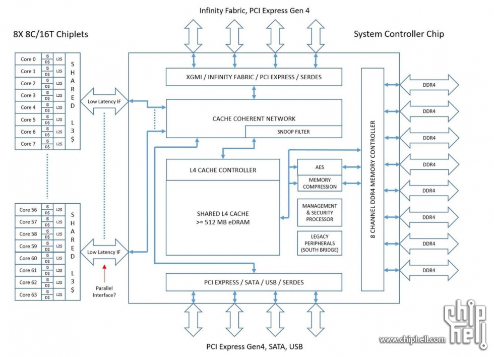
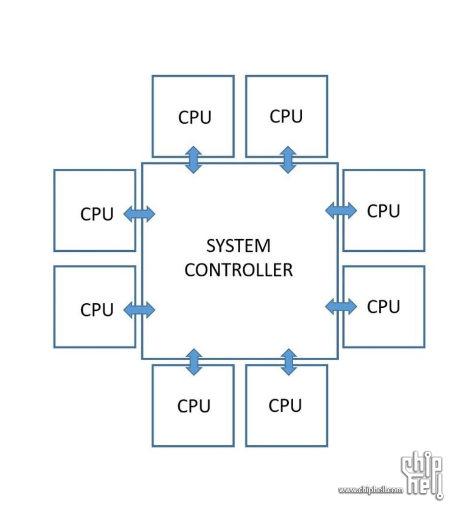
Interestingly, the system controller chip can be fabbed at gloflo at 12nm to help with the volume agreement.
Interestingly, the system controller chip can be fabbed at gloflo at 12nm to help with the volume agreement.
Latency to RAM would be ... interesting. Cache coherent network gets really prominent billing. 8 channels of DDR4 is specified, but number of PCIE4 (!) channels is not. Apparently the Legacy Peripherals aren't attached, and the secure processor is secured by being entirely unreachable ") Memory compression? Isn't that normally a video card thing?
Memory compression? Isn't that normally a video card thing?
Memory compression? Isn't that normally a video card thing?Vattila
Senior member
- Oct 22, 2004
- 799
- 1,351
- 136
it also means 8C/16T CCXs.
If so, it will be interesting to see how the cores are wired up, i.e. what the interconnect topology looks like. Same goes for the topology for the chiplets. It is certainly no longer direct-connection for 8 cores, nor for 8 chiplets.
If so, it will be interesting to see how the cores are wired up, i.e. what the interconnect topology looks like. Same goes for the topology for the chiplets. It is certainly no longer direct-connection for 8 cores, nor for 8 chiplets.
More than that, where is the edram? this leads me to belive there will be 256mb of edram on a CCX.
coercitiv
Diamond Member
- Jan 24, 2014
- 6,205
- 11,916
- 136
I came to this thread looking for Zen 2 EPYC details and all I got was this old empire interstellar dreadnought class schematic.
NTMBK
Lifer
- Nov 14, 2011
- 10,239
- 5,024
- 136
Urgh, I really hope this isn't true. Making every access to memory require an infinity fabric hop isn't going to help things.
Glo.
Diamond Member
- Apr 25, 2015
- 5,711
- 4,558
- 136
LOLOLOLOLOLOL.
https://twitter.com/chiakokhua/status/1041487772429705216
And https://twitter.com/peresuslog/status/1041514114789597185
Move on, nothing to see here.
And guys remember, Matisse IS 8C/16T design. That is one thing sure, at this moment.
https://twitter.com/chiakokhua/status/1041487772429705216
And https://twitter.com/peresuslog/status/1041514114789597185
Move on, nothing to see here.
And guys remember, Matisse IS 8C/16T design. That is one thing sure, at this moment.
NTMBK
Lifer
- Nov 14, 2011
- 10,239
- 5,024
- 136
LOLOLOLOLOLOL.
https://twitter.com/chiakokhua/status/1041487772429705216
And https://twitter.com/peresuslog/status/1041514114789597185
Move on, nothing to see here.
And guys remember, Matisse IS 8C/16T design. That is one thing sure, at this moment.
Phew.
LOLOLOLOLOLOL.
https://twitter.com/chiakokhua/status/1041487772429705216
And https://twitter.com/peresuslog/status/1041514114789597185
Move on, nothing to see here.
And guys remember, Matisse IS 8C/16T design. That is one thing sure, at this moment.
While I agree that this is BS. Also not sure how that diagram would prove 8c CCX's. Since when has Matisse been 8c16t been a sure thing? I don't think I have seen anything to say as much.
moinmoin
Diamond Member
- Jun 1, 2017
- 4,952
- 7,665
- 136
Aside that everything is BS anyway, I think some form of transparent real time memory/transport compression is overdue to alleviate any bandwidth congestion (most advantageous both in bandwidth limited high core MCMs like TR2 and in APUs).Memory compression? Isn't that normally a video card thing?
Vattila
Senior member
- Oct 22, 2004
- 799
- 1,351
- 136
The diagram is not credible at all, none of this makes any sense.
Can you please elaborate?
You sound confidently knowledgeable, but your assertion makes me none the wiser.
In my view, as a non-expert, much of the diagram makes sense, e.g. 8 memory channels are expected, level 4 cache seems reasonable, AES for memory encryption is expected, memory compression seems reasonable, security processor is a given, as is an integrated south-bridge, and the 9-chiplet design accords with rumours (AdoredTV, Twitter chatter).
The two things my suspicion reacted to were the 8-core chiplet with shared L3 (implying an 8-core CCX, which I very much doubt, and which conflicts with SemiAccurate's reporting), as well as the red arrow pointing to the "Low Latency IF" with the annotation "Parallel interface?". The latter in particular seemed suspect.
Last edited:
Vattila
Senior member
- Oct 22, 2004
- 799
- 1,351
- 136
And guys remember, Matisse IS 8C/16T design. That is one thing sure, at this moment.
Do you have a source for that?
By the way, I think Charlie from SemiAccurate has tweeted that the 8-core chiplets have two 4-core CCXs, just as before. Is that your source?
french toast
Senior member
- Feb 22, 2017
- 988
- 825
- 136
NostaSeronx
Diamond Member
- Sep 18, 2011
- 3,686
- 1,221
- 136
L3 cache is on-die SRAM. => 2 TB/s per CCX?
L4 cache is 3D stacked SRAM. => 1 TB/s per two CCXs?
L5 cache is 2.5D stacked HBM3 => 512 GB/s per CPU?
If you want to inflate the ASP of such things.
CPU + HBM => 200 mm squared.
Stacked SRAM => No die area penalty.
Maintains compatibility with existing solutions, but might swap to another substrate/interposer for higher density I/O capability.
GMI/xGMI assist goes to the HBM dies rather than the SRAMs.
Last edited:
Olikan
Platinum Member
- Sep 23, 2011
- 2,023
- 275
- 126
Qualcomm uses... page 16-17Memory compression? Isn't that normally a video card thing?
https://www.google.com.br/url?sa=t&...FjAAegQIABAB&usg=AOvVaw1UMP1wTQcVkzukxQt0rRII
DrMrLordX
Lifer
- Apr 27, 2000
- 21,634
- 10,850
- 136
For a minute there, it was like AMD was trying to make their own OpenPOWER CPU. Who knows, maybe they are . . .
chiplets!
I was thinking, the other day, that it would be wise for AMD to move away from 4-core CCXs to 8-core CCXs, assuming they could keep intracore latency the same. That way the consumer parts (Matisse) could be 1 CCX 8c/16t, avoid the inter-CCX latency penalty, and gain a big boost in a lot of apps currently not well-optimized for Zen/Zen+.
Gideon
Golden Member
- Nov 27, 2007
- 1,644
- 3,694
- 136
With up to 8 cores it would probably make sense to use a ring-bus within the chiplet, as intel does. This would also allow unified L3 cache usage.I was thinking, the other day, that it would be wise for AMD to move away from 4-core CCXs to 8-core CCXs, assuming they could keep intracore latency the same. That way the consumer parts (Matisse) could be 1 CCX 8c/16t, avoid the inter-CCX latency penalty, and gain a big boost in a lot of apps currently not well-optimized for Zen/Zen+.
Either way they will take some hits. Either a uniform one with every core-to-core connection (mesh), a small one with cores more than 1 hop away (Ringbus) or a bigger one between different core-complexes (CCX). There are no free lunches.
They could also just improve the latency between CCXes, keeping the high-level architecture as-is, because it's ridiculously horrible right now. On-chip CCX latency is 2/3 of the latency between two separate dies (connected via slow MCM connections) Its also more than the memory latency.
DrMrLordX
Lifer
- Apr 27, 2000
- 21,634
- 10,850
- 136
They could also just improve the latency between CCXes, keeping the high-level architecture the same as it's ridiculously horrible right now (2/3 of the latency between two dies and more than the memory latency)
They sort-of have to. Look at the latency numbers on the 2990WX and similar. Scary stuff.
The bad part about it is that as core counts go up, the share of power consumption granted to IF-related hardware goes wayyyyyyyyyy up, without even taking into account what happens when you start upping those IF clocks.
I am really, really hoping we get fully-tweakable IF speeds in Matisee and/or robust support for DDR4-4000 (or faster!) modules so we can get those IF clocks up high. The power usage penalty for high IF clocks shouldn't be too high on 8c Matisse.
Glo.
Diamond Member
- Apr 25, 2015
- 5,711
- 4,558
- 136
If AMD will shy away from 4 core CCX it will mean that there will be no more NUMA and no more CCX design.For a minute there, it was like AMD was trying to make their own OpenPOWER CPU. Who knows, maybe they are . . .
chiplets!
I was thinking, the other day, that it would be wise for AMD to move away from 4-core CCXs to 8-core CCXs, assuming they could keep intracore latency the same. That way the consumer parts (Matisse) could be 1 CCX 8c/16t, avoid the inter-CCX latency penalty, and gain a big boost in a lot of apps currently not well-optimized for Zen/Zen+.
It will be pretty interesting design, after all, to be honest.
TRENDING THREADS
-
-
 Discussion Intel current and future Lakes & Rapids thread
- Started by TheF34RChannel
- Replies: 23K
-
 Discussion Zen 5 Speculation (EPYC Turin and Strix Point/Granite Ridge - Ryzen 9000)
- Started by DisEnchantment
- Replies: 10K
-
 Discussion Speculation: Zen 4 (EPYC 4 "Genoa", Ryzen 7000, etc.)
- Started by Vattila
- Replies: 13K
-
Discussion Intel Meteor, Arrow, Lunar & Panther Lakes Discussion Threads
- Started by Tigerick
- Replies: 7K
AnandTech is part of Future plc, an international media group and leading digital publisher. Visit our corporate site.
© Future Publishing Limited Quay House, The Ambury, Bath BA1 1UA. All rights reserved. England and Wales company registration number 2008885.