2013 core sizes: A7-A15-Jaguar-Atom-Haswell

Page 6 - Seeking answers? Join the AnandTech community: where nearly half-a-million members share solutions and discuss the latest tech.

IntelUser2000

Elite Member
Oct 14, 2003
8,686
3,785
136
Looks like Cortex-A15 in the implementations we have any real info on is about 1.5W/core @ 1.7GHz in Exynos 5250 (Samsung 32nm) and 1.3W/core @ 1.8GHz in Exynos Octa (Samsung 28nm). That probably varies tangibly with bins. I don't think it'll need more than 1.2GHz to be competitive with 1GHz Jaguar cores, and it'll probably need substantially less than peak power to reach that.. as I've always been saying we really need actual perf/W curves to really make a valid comparison, you can't just look at peak vs peak when the peaks represent different perf levels.

The real question is how much power the non-core functions consume. Looks like at 1.2GHz the Exynos is using close to 3W for the core, while the 5.9W TDP for Jaguar is basically max power. I'll test Dhrystone out for cpu power use(using HWINFO) both on my IVB Ultrabook and the Clover Trail Tablet(that depends on whether Clover Trail device has enough sensors for that though).
 
Last edited:

Exophase

Diamond Member
Apr 19, 2012
4,439
9
81
The real question is how much power the non-core functions consume. Looks like at 1.2GHz the Exynos is using close to 3W for the core, while the 5.9W TDP for Jaguar is basically max power.

Where are you getting that from? And what do you mean by core? The CPUs? It's pretty much 3W for max for both CPU cores at 1.7GHz. Whatever the GPU uses under any circumstances has nothing to do with this.
 

IntelUser2000

Elite Member
Oct 14, 2003
8,686
3,785
136
Where are you getting that from? And what do you mean by core? The CPUs? It's pretty much 3W for max for both CPU cores at 1.7GHz. Whatever the GPU uses under any circumstances has nothing to do with this.

I'm talking about 3W for the quad core Exynos(Exynos Octa) running at 1.2GHz, since you mentioned that frequency.

Actually, I did pixel counting in paint and got 2.6W at 1.2GHz(16800MIPS).

Anyways, the Clover Trail system I have does not have the sensors for the CPU but the Ivy Bridge Ultrabook does. Some interesting results here.

At 2.8GHz frequency:

-55200MIPS in Dhrystone
-14.2W max package power, 12W core power for a certain duration(my system has the CPU set at 15W), with 12.5W package power, 10.2W core power for remainder of the benchmark

At 800MHz LFM locked:

-15500MIPS
-5W package power, 2.8xW core power for a certain duration, with 4.5W package power and 2.4xW core power for the remainder of the time

(The GPU power use is insignificant at 2-10mW and the non-core functions vary little at 2-2.3W)

I also find it interesting how little it uses at 800MHz. 5W package power in Dhrystone probably means if its capped at that frequency, 7W SDP is realistic even under load(but SDP is for another topic). Also the little variation of non-core power(package power - core power - gpu power) means it doesn't really do much of power management and puts an absolute ceiling on how low they can go with TDP.
 
Last edited:

Exophase

Diamond Member
Apr 19, 2012
4,439
9
81
I'm talking about 3W for the quad core Exynos(Exynos Octa) running at 1.2GHz, since you mentioned that frequency.

Actually, I did pixel counting in paint and got 2.6W at 1.2GHz(16800MIPS).

Right, 2.6W for 4 cores at 1.2GHz, or < 0.7W per core. It remains to be seen if that's really what you get, but that's not really bad at all. I really doubt Temash will actually use < 3W for the CPU cores at 1GHz. I know that it has other stuff on the SoC. But if the TDP is nearly 6W yet it can't even allocate half of that to the CPU when the GPU is barely doing anything then its turbo is doing a poor job or it doesn't have turbo at all except for when the docking station says it's okay.

Anyways, the Clover Trail system I have does not have the sensors for the CPU but the Ivy Bridge Ultrabook does. Some interesting results here.

At 2.8GHz frequency:

-55200MIPS in Dhrystone
-14.2W max package power, 12W core power for a certain duration(my system has the CPU set at 15W), with 12.5W package power, 10.2W core power for remainder of the benchmark

At 800MHz LFM locked:

-15500MIPS
-5W package power, 2.8xW core power for a certain duration, with 4.5W package power and 2.4xW core power for the remainder of the time

(The GPU power use is insignificant at 2-10mW and the non-core functions vary little at 2-2.3W)

I also find it interesting how little it uses at 800MHz. 5W package power in Dhrystone probably means if its capped at that frequency, 7W SDP is realistic even under load.

Just going to ignore the DMIPS stuff, it's a useless awful benchmark :p

So you're saying at 800MHz the two cores (both were active right?) only used 2.4-2.8W, but the whole package used 4.5W - and most of that wasn't GPU? Then what on earth was it? I don't think the memory controller should be using anywhere close to that, nor L3..
 

IntelUser2000

Elite Member
Oct 14, 2003
8,686
3,785
136
Just going to ignore the DMIPS stuff, it's a useless awful benchmark :p

So you're saying at 800MHz the two cores (both were active right?) only used 2.4-2.8W, but the whole package used 4.5W - and most of that wasn't GPU? Then what on earth was it? I don't think the memory controller should be using anywhere close to that, nor L3..

The whole point of using DMIPS is because Samsung used it. It also proves that there are high load applications that does not load it to TDP.

Also, yes, the uncore functions can use that much power. Because that's what the Datasheet for Ivy Bridge chip says it as well. For Package C7, its rated at 2.2W for the 17W chips. But it seems its basically fixed regardless of frequency or load!
 

Exophase

Diamond Member
Apr 19, 2012
4,439
9
81
Just because Samsung used it doesn't mean it's useful for anything beyond trying to determine the frequency at the respective points. No matter what you think of a product nothing really justifies using DMIPS for marketing. Sadly a lot of companies still do it.

I'd argue that it doesn't necessarily even constitute as good representation of full CPU load, even if it uses 100% CPU time, because it doesn't cache miss at all. A normal application will be running the prefetchers hard but this one will barely touch them.
 

IntelUser2000

Elite Member
Oct 14, 2003
8,686
3,785
136
Just because Samsung used it doesn't mean it's useful for anything beyond trying to determine the frequency at the respective points. No matter what you think of a product nothing really justifies using DMIPS for marketing. Sadly a lot of companies still do it.

I'd argue that it doesn't necessarily even constitute as good representation of full CPU load, even if it uses 100% CPU time, because it doesn't cache miss at all. A normal application will be running the prefetchers hard but this one will barely touch them.

That applies same to the flash heavy browsing you are talking about. Those usage scenarios with sporadic demand doesn't let it go to TDP.

I'd also argue in Whetstone(FP) its where it reaches the higher point of the power usage as in my data, with lower one being reached by Dhrystone.
 

IntelUser2000

Elite Member
Oct 14, 2003
8,686
3,785
136
Looks like Intel caught up with the ARM cores in core size even if we normalize for process:

http://www.expreview.com/39814.html

64% reduction from 22nm Silvermont. According to Anandtech, A15 @ 28nm is 2.74mm and 20nm is 1.67mm. 14nm Airmont is at 0.82mm2. Even if we assume 50% reduction, we get 0.835mm2 for hypothetical 14nm A15. Now we did not at 20nm, we got a 39% reduction, and 14nm is actually even worse. If we assume 60% scaling for 14nm, we'd end up with a 1mm2 A15 and that's 22% larger than Airmont. Looks like Intel might actually beat them in their claims that its 35% more dense.

Also we have a record L2 cache density: 1mm2/MB. At 22nm its 2.3mm2.
 
Last edited:

witeken

Diamond Member
Dec 25, 2013
3,899
193
106
Looks like Intel caught up with the ARM cores in core size even if we normalize for process:

http://www.expreview.com/39814.html

64% reduction from 22nm Silvermont. According to Anandtech, A15 @ 28nm is 2.74mm and 20nm is 1.67mm. 14nm Airmont is at 0.82mm2. Even if we assume 50% reduction, we get 0.835mm2 for hypothetical 14nm A15. Now we did not at 20nm, got got a 39% reduction, and 14nm is actually even worse. If we assume 60% scaling for 14nm, we'd end up with a 1mm2 A15 and that's 22% larger than Airmont. Looks like Intel might actually beat them in their claims that its 35% more dense.

Also we have a record L2 cache density: 1mm2/MB. At 22nm its 2.3mm2.
A15 probably has more transistors.
 

erunion

Senior member
Jan 20, 2013
765
0
0
Looks like Intel caught up with the ARM cores in core size even if we normalize for process:

http://www.expreview.com/39814.html

64% reduction from 22nm Silvermont.


1-1080.3935632552-9621d45d0d4dce0a.jpg


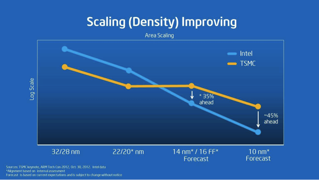
The aggressive scaling immediately made me think of this slide.


8857531-1394569477766125-Jeff-Groff.png


It will be interesting to see who's version turns out to be the truer.
 

Exophase

Diamond Member
Apr 19, 2012
4,439
9
81
Looks like Intel caught up with the ARM cores in core size even if we normalize for process:

http://www.expreview.com/39814.html

64% reduction from 22nm Silvermont. According to Anandtech, A15 @ 28nm is 2.74mm and 20nm is 1.67mm. 14nm Airmont is at 0.82mm2. Even if we assume 50% reduction, we get 0.835mm2 for hypothetical 14nm A15. Now we did not at 20nm, got got a 39% reduction, and 14nm is actually even worse. If we assume 60% scaling for 14nm, we'd end up with a 1mm2 A15 and that's 22% larger than Airmont. Looks like Intel might actually beat them in their claims that its 35% more dense.

Also we have a record L2 cache density: 1mm2/MB. At 22nm its 2.3mm2.

But on the other hand we have Exynos 7420 at 78mm^2 vs Exynos 5433 at 118mm^2, despite the former likely having significantly more transistors at least in the GPU. This is for a node change that was supposed to only be slightly denser (~15%) or not smaller at all (according to Intel and some others). It looks like maybe some offerings on Samsung's 20nm weren't really living up to their density potential and the 14nm process picked up some of the slack, but that's really just a guess. We should be able to work out A57 core size in Exynos 7420 soon, so maybe that'll be another useful data point in your comparison. Disregarding that A57 isn't A15.

Ashraf measures about 87mm^2 for Cherry Trail (http://www.fool.com/investing/gener...rporation-cherry-trail-die-size-revealed.aspx), we'll still have to see how its GPU and CPU perf and perf/W compare with Exynos 7420, but at first glance it looks like Samsung is doing pretty well density-wise for a chip on what's supposed to be a significantly less dense process.
 
Last edited:

AtenRa

Lifer
Feb 2, 2009
14,001
3,357
136
1-1080.3935632552-9621d45d0d4dce0a.jpg


The aggressive scaling immediately made me think of this slide.


8857531-1394569477766125-Jeff-Groff.png


It will be interesting to see who's version turns out to be the truer.

So if going from 28nm to 14nm on the ARM CPU will net a 64% smaller size, then both will be correct :p
 

erunion

Senior member
Jan 20, 2013
765
0
0
So if going from 28nm to 14nm on the ARM CPU will net a 64% smaller size, then both will be correct :p

Click the link in the word "version". TSMC made a rebuttal slide that varied from Intel's slide.

Someone has to be wrong.
 

witeken

Diamond Member
Dec 25, 2013
3,899
193
106
Ashraf measures about 87mm^2 for Cherry Trail (http://www.fool.com/investing/gener...rporation-cherry-trail-die-size-revealed.aspx), we'll still have to see how its GPU and CPU perf and perf/W compare with Exynos 7420, but at first glance it looks like Samsung is doing pretty well density-wise for a chip on what's supposed to be a significantly less dense process.
So Broxton (~58mm²) is smaller than Cherry Trail.

http://seekingalpha.com/article/1882851-intels-broxton-die-size-revealed
 

witeken

Diamond Member
Dec 25, 2013
3,899
193
106
That die size for Broxton was nonsense from the beginning. I told it and people denied it.
Intel said it is to scale, so your comment is irrelevant.

Edit: unless the relative die area is only true on the vertical axis, then Broxton would 75% of Bay Trail (ratio height BT and BXT instead of ratio area), which would be 76mm².
 
Last edited:

Mortius

Junior Member
Dec 4, 2013
14
0
0
Click the link in the word "version". TSMC made a rebuttal slide that varied from Intel's slide.

Someone has to be wrong.

TSMC badged slide stating that 16nm is 10% denser than 20nm

I suspect that part of the problem may be because of TSMC's decision to have two "16nm" nodes. Intel's slide shows a comparison against 16FF with its marginal improvement. TSMC's slide is using their 16FF+ process which improves the density somewhat.

At this point Samsung comes along and muddies the water even further. Samsung has called its version of 16FF+ their 10nm process, which reportedly has SRAM cells that are only marginally denser than Intel's 14nm.

For the cynical, the solution to Intel's apparent process technology advantage is better marketing, not more research and development.
 

witeken

Diamond Member
Dec 25, 2013
3,899
193
106
It doesn't matter since the comparison is theoretical: it compares feature sizes. Who says Intel hasn't already got a similar 15% density from going FinFET?

BTW, this is the latest version:

15650137820_be301f008c_b.jpg
 
Last edited:

Mortius

Junior Member
Dec 4, 2013
14
0
0
That die size for Broxton was nonsense from the beginning. I told it and people denied it. You should expect that Broxton gets another GPU increase and hopefully much improved CPU cores. Therefore, such a massive die reduction on the same process is wishful thinking.

Your credulity is rather lacking.

The secret to Broxton is taking Bay-Trail and scaling it down so that all of its components exist, but are proportionally smaller. To adapt it to a mid-range smartphone with inbuilt 4G is achieved by making everying proportionately smaller yet again. Swap out the radio for 3G and target cheaper phones and a lower power budget? Make everything smaller yet again.
 

mikk

Diamond Member
May 15, 2012
4,140
2,154
136
Intel said it is to scale, so your comment is irrelevant.


Intel also said Broxton is coming mid-2015, think logical about it and don't trust in every marketing slide and comment from Intel. Simply forget 58mm², this is nonsense.
 

witeken

Diamond Member
Dec 25, 2013
3,899
193
106
Intel also said Broxton is coming mid-2015, think logical about it and don't trust in every marketing slide and comment from Intel. Simply forget 58mm², this is nonsense.

TTM is something completely different.

Apparently you haven't read my edit.
 

AtenRa

Lifer
Feb 2, 2009
14,001
3,357
136
Looks like Intel caught up with the ARM cores in core size even if we normalize for process:

http://www.expreview.com/39814.html

64% reduction from 22nm Silvermont. According to Anandtech, A15 @ 28nm is 2.74mm and 20nm is 1.67mm. 14nm Airmont is at 0.82mm2. Even if we assume 50% reduction, we get 0.835mm2 for hypothetical 14nm A15. Now we did not at 20nm, got got a 39% reduction, and 14nm is actually even worse. If we assume 60% scaling for 14nm, we'd end up with a 1mm2 A15 and that's 22% larger than Airmont. Looks like Intel might actually beat them in their claims that its 35% more dense.

Also we have a record L2 cache density: 1mm2/MB. At 22nm its 2.3mm2.


Intel 32nm Clovertrail core die size = 5.6mm^2
Intel 22nm(50% reduction) Baytrail core die size = ~2.8mm^2

With 64% reduction from 14nm, Airmont core die size should be close to ~1.01mm^2

How did you come to 0.82mm^2 ???
 
Last edited: