I find it quite intriguing that AMD is able to contain so much of the bandwidth requirements using on die L2s, to the point that AMD can get away with LPDDR memory.
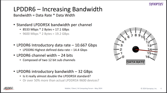
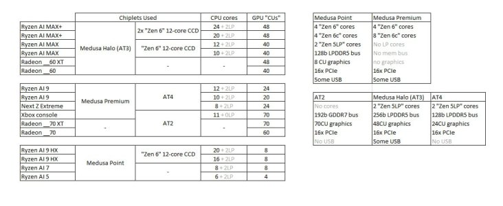
LPDDR6 is very fast even with early spec. AT3 with 384bit quad channel LPDDR6 @12Gbps has 576GB/s memory BW. Half-way between 4070 TI and 9070XT. Should be plenty with nextgen clean slate RDNA 5 µarch and ISA and unified L2 and MALL like NVIDIA.
Still wondering how big that L2 will be on AT3 and AT4. 20MB seems too low, but perhaps they'll beef up wiring and cache control circuitry like they did with RDNA 4 and even 32MB might be enough.
AMD could be trolling NVidia on low end with big LPDDR5 memory sizes.
What I wonder though, why not doe the same throughout the stack?
If NVidia can go up to 512 bit memory bus (8 channels) why not go to 6 LPDDR6 channels with high end card, which would be 576 bits?
Because then, if the biggest LPDDR5 memory chip is 64 GB, the high end professional / AI card could have 384 GB, which would be maximum trolling.
Or maybe split high end gaming to use GDDR7 and high end professional / AI with LPDDR6.
But, it's also good to keep in mind that NVidia is also doing a lot of work with LPDDR across the product stack, so AMD may not have a monopoly here.
There's no need. 4GB modules over 192bit = 24GB, so doubt PS6 will go any higher. 24GB seems like the sweet spot.
Gaming stack could look like this
AT0 36/48GB
AT2 24GB
AT3 24/32GB
AT4 12/16GB
At some point LPDDR6 PHYs become comically large and GDDR7 makes more sense. Maybe a split memory controller design (LPDDR6 + GDDR7) but that will probably be too much work.
AT3 can already tap out at 512GB without clamshell. 64GB x 8 = 512GB. 576bit would be 768GB.
Datacenter and very high end professional will probably lean into some other tech like HBF in addition to HBM, but we'll see.
Yeah isn't N1X and N1 using LPDDR5X?