Why does Intel pick particular node sizes?

ehume

Golden Member
Nov 6, 2009
1,511
73
91
OK. I know that node sizes are chosen for marketing reasons, and don't actually represent the actual sizes of any features, still those numbers are supposed to stand for something.

Now, as far back as I know, the node sizes are 65nm, 45nm, 32nm, 22nm and 14nm, with
10nm and 7nm yet to come. I have seen 28nm and 20nm referred to as "half nodes." I can see that from 65nm to 22nm each step represented a shrinkage of sqrt(2) until we reach 14nm. The continuity breaks there.

Worse, this is all supposed to have derived from a master size of 193nm, the wavelength of blue light. But on a little spreadsheet I cannot reach the current series unless I do 193nm/3 to get 64.33nm. And I seem to recall there were 135nm and 95nm node sizes (I may be remembering those incorrectly). Those don't fit very well.

Can someone please list the correct node sizes, and explain why they were chosen?
 

BSim500

Golden Member
Jun 5, 2013
1,480
216
106
Last edited:

witeken

Diamond Member
Dec 25, 2013
3,899
193
106
The 193nm you're referring to isn't a feature size. It's the wavelength of light that's being used for the lithography.

This is Intel's 14nm node:

14nmFeatureSize.png


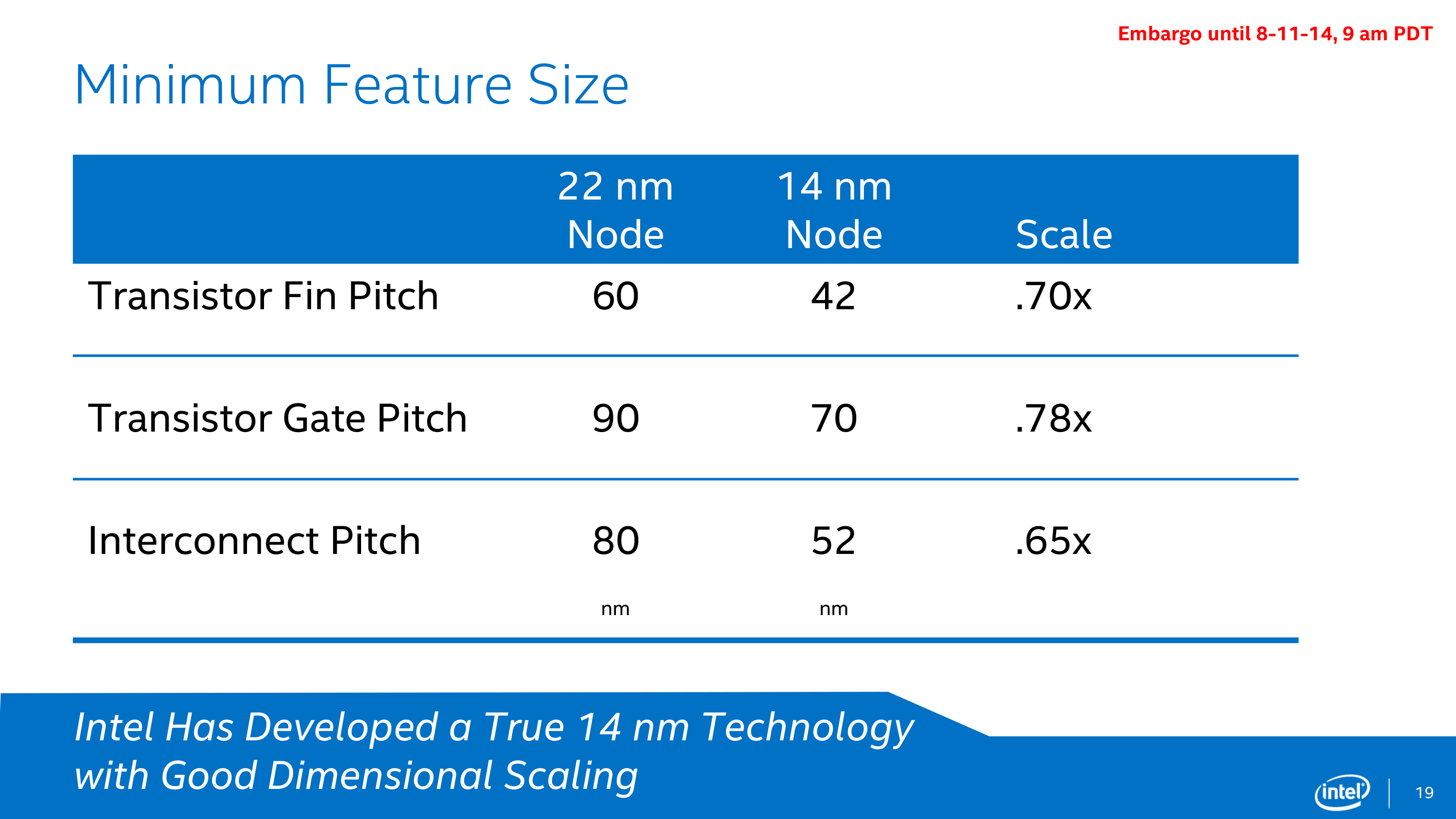
Those are the smallest transistors you're going to find until the 10nm node arrives. So indeed it's just marketing: when a company creates a new process, they give it the name that is about 1.4x smaller. But often the density doesn't increase by 2x, so the node names becomes smaller than the real transistor. For example, Intel's 32->22 node should be 2.1x shrink according to the name, but it's a 1.7x shrink or so. Intel's 22->14 is a 2.2x shrink instead of 2.5x.

The particular reason why Intel went with 14nm instead of 16nm, is because Intel did an effort to gain a density lead at 14nm. Historically Intel has been focusing more on performance instead of density for obvious reasons, but they wanted to continue the cost/transistor scaling. Because wafer cost rises faster now, they need to increase density more than usually.

I don't think I can give you the "real" names since those don't exist. What I can do, however, is give you a sense of how the nodes compare:

15650137820_be301f008c.jpg


Intel's 14nm is -- theoretically -- 1.5x more dense than other people's 14/16nm and 20nm.
 
Last edited:

Idontcare

Elite Member
Oct 10, 1999
21,118
58
91
OK. I know that node sizes are chosen for marketing reasons, and don't actually represent the actual sizes of any features, still those numbers are supposed to stand for something.

Now, as far back as I know, the node sizes are 65nm, 45nm, 32nm, 22nm and 14nm, with
10nm and 7nm yet to come. I have seen 28nm and 20nm referred to as "half nodes." I can see that from 65nm to 22nm each step represented a shrinkage of sqrt(2) until we reach 14nm. The continuity breaks there.

Worse, this is all supposed to have derived from a master size of 193nm, the wavelength of blue light. But on a little spreadsheet I cannot reach the current series unless I do 193nm/3 to get 64.33nm. And I seem to recall there were 135nm and 95nm node sizes (I may be remembering those incorrectly). Those don't fit very well.

Can someone please list the correct node sizes, and explain why they were chosen?

In the beginning, go back to the 10um and 3um days, the node label directly referred to the length of the transistor gate (what we laypeople think of as being the width of the transistor gate when we see the fancy cross-section SEM images in marketing materials).

Eventually this morphed into the width of the drawn gate, then the width of the drawn channel, then the width of the effective channel (different than drawn because of resist trimming, HALO implantations, etc). And at one point (for logic anyways, still is true for memory) was used to refer to 1/2 the contacted gate pitch, and then 1/2 the minimum metal pitch.

Nowadays it pretty refers to nothing, it has become a "generation XYZ" type marketing moniker.

But the reason Intel (or any other company) picks a specific number for their node label, say 22nm versus 20nm, or 14nm versus 16nm, comes down to mathematics and tradition and basically is intended to loosely capture the areal shrink benefits of going from node N to node N+1.

If the areal shrink benefits are 50% (entitlement, not actual) then you typically captured that and communicated by taking your node label and multiplying by 0.7x.

For Intel that means 22nm * 0.7 = 15nm

And for a while Intel did refer to their node after 22nm as being the 15nm node. But then the R&D guys went a little more aggressive on the areal shrink factor, making all the tighter metal and fin pitches, and enabling a 43% shrink entitlement versus 50%.

22nm * 0.65 = 14 nm

And so they adjusted their node label to reflect the better than expected areal shrink entitlement.

But the numbers 22nm and 14nm stem from days of yore, if you back out all the nodes you will eventually get to the ones that had node labels which meant something physical, and each one thereafter delivered roughly the areal shrinkage one would expect based on straight physical scaling even though the straight physical scaling was no longer happening.
 

ehume

Golden Member
Nov 6, 2009
1,511
73
91
@BSim500 - Thanks for finding the Wikipedia article I was looking for and did not find.
@witiken - Thanks for the perspective.
@Phynaz - so droll
@IDC - Thanks for a clear statement of why the numbers were chosen. As I suspected, it's a nice balance of reality and marketing. I'll sleep easier at night.:D