
TMSC got onto an alternate schedule when they went from 65nm to 55nm, but since then they've been keeping the full node cadence.I am confused. 55nm to 28nm is a half-node + full-node (1.5 full node steps):
55nm -> 40nm (half node)
40nm -> 28nm (full node)
28nm -> 20/22nm (half node)
28nm -> 14/16nm (full node)
http://www.decryptedtech.com/leaks-...f-node-and-move-straight-to-16nm-for-new-gpus
How are you getting 2 steps? It's the same as moving from 40nm to 28nm (Kepler to Maxwell) or 1 full node. Is it not?
TSMC's description also coicides with just a 1 full node shrink:
"TSMC's 16FF+ (FinFET Plus) technology can provide above 65 percent higher speed, around 2 times the density, or 70 percent less power than its 28HPM technology."
A 2 node step would result in more than 2X the density increase and more than a 70% reduction in power usage/more than 65% increase in transistor switching speed. This coincides with rumours that next gen flagship chips will have 16-18B transistors, which is about double of the existing GM200/Fiji chips.
1.5 node steps would be 28nm -> 10nm (14/16nm is full node + 1/2 node to 10nm), while 2 full node steps is 28nm -> 7nm.
---
GTX285 (55nm) had 1.4B transistors.
GTX780Ti (1st gen 28nm) had 7.1B (5X 285's)
GTX980Ti (28nm) had 8B (5.7X).
Granted, there will be other benefits such as HBM2/GDDR5X (higher memory bandwidth) and possible improvements in IPC/compute/DX12 capability via a newer architecture. I don't think NV will launch a consumer $699 card 80-100% faster than a 980Ti in 2016. Why would they when they can just split the generation into parts or first release a Titan X successor for $1K+?
55nm to 40nm was a full node. 55/40 = 1.428 = ~√2
40nm to 28nm was also a full node. 40/28 = 1.428 = ~√2
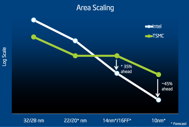
28nm to 20nm was the full node, but that didn't work out. 14nm would be the next full node from 20nm, so 28nm to 14nm would be two full nodes.
The difficulty arises when your full nodes no longer double your density, like they've seen with their "16nm" node. 28nm to 16/14nm should ideally give 4x the density, but we're not seeing that at all.
Edit: 22nm for Intel and 16nm for TMSC also introduced Finfet, which kind of breaks traditional scaling.
Last edited:
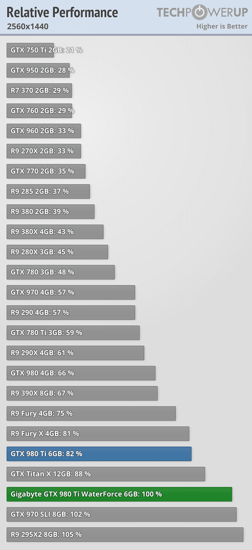
 That the 980 is so much faster is pretty amazing, and shows just how good Maxwell 2 is. The 980 has 47% more transistors than GK104 and 33% more cores, but performs much better than that.