[VideoCardz] NVIDIA PCB w/ Micron GDDR6

EXCellR8

Diamond Member
Sep 1, 2010
3,982
839
136
Just a prototype obviously, but interesting nonetheless

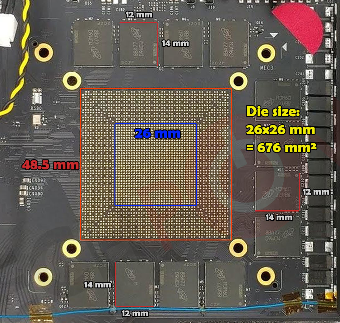
This board lacks actual GPU, which appears to be rather large (add 12GB memory and we have a new enthusiast SKU). These boards are used for testing, which is demonstrated by tens of switches and connectors. It’s where the development starts, so it’s not exactly clear how this picture got leaked.

There is no need to jump into conclusion that this is GeForce product. This could very well be Quadro or next-gen Tesla. Most of them share the same board design anyway.

Source
 

crisium

Platinum Member
Aug 19, 2001
2,643
615
136
The only useful thing here is that Nvidia has 14Gbps GDDR6 chips on hand. So that's likely a floor of where GDDR6 will begin on the next gen.
 

EXCellR8

Diamond Member
Sep 1, 2010
3,982
839
136
With twelve chips, this board has a 384-bit memory bus and 12 GB VRAM. The memory bandwidth at 14 Gbps data rate is a staggering 672 GB/s, which conclusively beats the 484 GB/s that Vega 64 and GTX 1080 Ti offer.

not without a GPU it doesn't :D

like another user pointed out this PCB doesn't even have video outputs, except for maybe a LCD ribbon at the top left I noticed? strikes me as a test mule that is being used to dial in the memory and test out the limitations. and yea 3x 8pin connectors but that doesn't really have any merit except for maybe load testing.
 

Det0x

Golden Member
Sep 11, 2014
1,028
2,953
136
https://www.techpowerup.com/245501/...potted-up-to-525-w-power-delivery-gtx-1180-ti

6uws0zn3v0cXaOSk.jpg


I tried to estimate die size from the photo. We do know from the datasheet that the GDDR6 memory chips are 14 mm x 12 mm. Based on that information I rescaled, warped and straightened the image, so that each GDDR6 memory chip is 140 x 120 pixels. With all memory chips around the GPU now being at the correct size, we can use the GPU's silkscreen print to estimate the actual size of the chip package, which I measured at 48.5 x 48.5 mm. Assuming that the inner silk screen with the solder balls represents the surface of the GPU die, we get a length of 26 mm for each side of the die, which brings die size to 676 mm².

Confirms TSMC 12nm FFN as there is no way they could go this big on a ramping 7nm node for anything other then their HPC margins, and those cards use hbm2.

Predict the Geforce 11x0 series will be short lived, since Nvidia will release TSMC 7nm gaming cards next year.
 

LTC8K6

Lifer
Mar 10, 2004
28,520
1,575
126
Yeah, just a memory test mule, so the die layout in the middle really doesn't mean anything as far as an upcoming GPU.
It doesn't tell us anything except that NV is testing GDDR6 ram, which we really already knew.
 

Bouowmx

Golden Member
Nov 13, 2016
1,138
550
146
1.4 * GV102 (in area, and likely, in number of cores, TMUs, and ROPs)

Exactly like I expected.

However, GP100 vs GV100 says area scaling isn't linear. Despite 1.4x the execution units, and Tensor cores, area is only 1.33x.
 

alcoholbob

Diamond Member
May 24, 2005
6,271
323
126
So it is in theory still possible that 1180 will be on 12nm and 1180ti could be 7nm.
 

EXCellR8

Diamond Member
Sep 1, 2010
3,982
839
136
I feel like they're gonna go straight to 2080/2070 series and not bother with 1100, 1200 etc.