TSMC 10nm details (TSMC Symposium)

witeken

Diamond Member
Dec 25, 2013
3,899
193
106
TSMC Symposium: “10nm is Ready for Design Starts at This Moment”

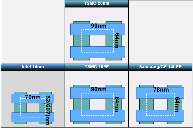
The good news is that scaling still works. Due to aggressive scaling, the 10nm FinFET (10FF) process node increases logic density by 2.1X compared to the TSMC 16nm FinFET Plus (16FF+) process node. Compared to 16FF+, the 10FF node can offer a 20% speed increase at the same power, or more than 40% power reduction at the same speed. TSMC has demonstrated a fully functional 256Mb SRAM in 10FF technology with die size scaling close to 50% of 16FF+.
New features in 10FF include a unidirectional (1D) layout style and new local interconnect layer. These features help 10FF achieve a 2.1X logic density improvement over 16FF+, whereas normally TSMC gets about a 1.9X density boost for node migration, Woo said. In addition to the density improvement, the 1D Mx architecture can reduce CD (critical dimension) variation by 60%, she said.
10FF requires double patterning, but TSMC does not use not the relatively simple litho-etch, litho-etch patterning that is used at 20nm and 16nm. The problem with LELE, Woo said, is that overlay changes can result in variation in the line space. While this is tolerable in 20nm and 16nm, at 10nm this variation will translate into a very small metal space. That can result in an immature dielectric breakdown. Thus, TSMC 10FF uses a self-aligned spacer process that assures that uniform metal line spacings are maintained.

Another 10nm challenge is that resistance goes up significantly as metal layers scale down. Selectively relaxing the metal pitch provides a way to optimize performance versus density. 10FF allows the designer to make this kind of adjustment in order to find the best tradeoff.
Also:

TSMC Symposium: New Low-Power Process, Expanded R&D Will Drive Vast Innovation: TSMC Executive

Moore’s Law “Not Slowing Down”—TSMC Executive
 

Fjodor2001

Diamond Member
Feb 6, 2010
3,786
256
126
So who does still consider TSMC 10 nm to be a 14 nm equivalent, and by what justification?
 

ShintaiDK

Lifer
Apr 22, 2012
20,378
145
106
TSMCs 16FF is 20nm. So TSMCs 10nm looks to be 14nm.

Cell-SizeComparison.png
 

Hans de Vries

Senior member
May 2, 2008
321
1,018
136
www.chip-architect.com
TSMCs 16FF is 20nm. So TSMCs 10nm looks to be 14nm.

Cell-SizeComparison.png

That image is pretty misleading in the sense that it suggest that
everybody uses simpler 1D interconnect. Everybody (except Intel)
was using much more complex 2D interconnect for their logic
processes for a good reason.

And it's not that they can't do small pitch 1D interconnect. Samsung
for example produced literally Billions of miles of 42nm and 46nm
1D interconnect with air gaps for its EVO 840 products.

That's many rotations of the Earth around the Sun.....

The big surprise is that TSMC now also goes to 1D interconnect
for it's 10nm Logic process:


TSMC symposium said:
New features in 10FF include a unidirectional (1D) layout style and new local interconnect layer. These features help 10FF achieve a 2.1X logic density improvement over 16FF+, whereas normally TSMC gets about a 1.9X density boost for node migration, Woo said. In addition to the density improvement, the 1D Mx architecture can reduce CD (critical dimension) variation by 60%, she said.

That means that at least we will be able to compare Apples to apples with
images such as the ones above:

TSMC symposium said:
The 10FF node, Woo said, can scale key pitches by more than 70%

So TSMS's 1D interconnect will be smaller than 0.7 times (the normal
scaling per node) I would expect gate/metal pitches shrinks to something
like 55nm/40nm

http://community.cadence.com/cadenc...0nm-is-ready-for-design-starts-at-this-moment
 

Exophase

Diamond Member
Apr 19, 2012
4,439
9
81
Who considers them to be not equivalent, and by what justification?

AFAIK TSMC's 20nm started out denser than Intel's 22nm, 16FF+ has an additional density improvement, and then both TSMC 16FF+ and Intel 22nm claim a 2.1x density improvement to the next node.. so how would that make TSMC 10nm equivalent in density to Intel 14nm? Is it taken as a great offence for TSMC to be rounded down to Intel's denser mode but it's totally fine to round it back to their less dense one? Sounds like a double standard.
 

Idontcare

Elite Member
Oct 10, 1999
21,118
58
91
AFAIK TSMC's 20nm started out denser than Intel's 22nm, 16FF+ has an additional density improvement, and then both TSMC 16FF+ and Intel 22nm claim a 2.1x density improvement to the next node.. so how would that make TSMC 10nm equivalent in density to Intel 14nm? Is it taken as a great offence for TSMC to be rounded down to Intel's denser mode but it's totally fine to round it back to their less dense one? Sounds like a double standard.

If the only metric of concern is maximum density (minimum pitch) in the absence of all other electrical and cost metrics, then there is no reason to not call TSMC's 10nm a 10nm (if not 9nm) node.

But if that were true, that density is the only (or the dominant) metric by which a node is valued, then all this other stuff relating to leakage, clockspeeds, power consumption, reliability, yields, design costs, production costs, capacity, cycle time, etc. must be one big bag of red herrings.
 
Apr 20, 2008
10,161
984
126
AFAIK TSMC's 20nm started out denser than Intel's 22nm, 16FF+ has an additional density improvement, and then both TSMC 16FF+ and Intel 22nm claim a 2.1x density improvement to the next node.. so how would that make TSMC 10nm equivalent in density to Intel 14nm? Is it taken as a great offence for TSMC to be rounded down to Intel's denser mode but it's totally fine to round it back to their less dense one? Sounds like a double standard.


If you're butthurt about this then you have no problems in your life and you should be thankful for it. The products on the node will speak for themselves, for better or worse.

Who cares what companies label their process as? It is an arbitrary number loosely defined by the companies themselves.
 

Exophase

Diamond Member
Apr 19, 2012
4,439
9
81
If you're butthurt about this then you have no problems in your life and you should be thankful for it.

Wow, I don't know what warranted a response like that. Are you sure I'm the one who's overreacting? Don't exactly think this is something I'm "butthurt" over, and one offhand remark on a forum is hardly a reflection of what bothers me in my life.

Just saying, some people are quick to (rightfully) point out that TSMC's processes no longer bear much relation to Intel processes of similar names, but that doesn't mean that TSMC is exactly aligned with Intel of one generation behind either.

The products on the node will speak for themselves, for better or worse.

Who cares what companies label their process as? It is an arbitrary number loosely defined by the companies themselves.

I agree.

If the only metric of concern is maximum density (minimum pitch) in the absence of all other electrical and cost metrics, then there is no reason to not call TSMC's 10nm a 10nm (if not 9nm) node.

But if that were true, that density is the only (or the dominant) metric by which a node is valued, then all this other stuff relating to leakage, clockspeeds, power consumption, reliability, yields, design costs, production costs, capacity, cycle time, etc. must be one big bag of red herrings.

Okay, but why should we assert that TSMC's 10nm will be like Intel's 14nm in any of those other metrics?
 
Last edited:
Mar 10, 2006
11,715
2,012
126
Okay, but why should we assert that TSMC's 10nm will be like Intel's 14nm in any of those other metrics?

TSMC 16FF has very similar drive currents, particularly at higher leakage levels, to Intel 22nm FWIW. At lower leakage levels, TSMC 16FF seems to be superior.
 

witeken

Diamond Member
Dec 25, 2013
3,899
193
106
AFAIK TSMC's 20nm started out denser than Intel's 22nm, 16FF+ has an additional density improvement, and then both TSMC 16FF+ and Intel 22nm claim a 2.1x density improvement to the next node.. so how would that make TSMC 10nm equivalent in density to Intel 14nm? Is it taken as a great offence for TSMC to be rounded down to Intel's denser mode but it's totally fine to round it back to their less dense one? Sounds like a double standard.

Intel doesn't claim, but Intel has proved that it can scale density by 2.2x.

In my opinion, TSMC should name its 10nm node 13nm (or maybe 12nm because Samsung/GloFo isn't going to go from 14->13). By doing that, TSMC will acknowledge

1) That it scaled density by a meager 2.4 (Cf. 20/13 ²) from 20->13.
2) That they have some density advantage versus Intel, but less dense than Intel's 10nm
3) That TSMC's 10nm isn't as advanced as Intel's 10nm because it lacks
*Air gaps
*III-V/Ge
 

NTMBK

Lifer
Nov 14, 2011
10,240
5,026
136
Intel doesn't claim, but Intel has proved that it can scale density by 2.2x.

In my opinion, TSMC should name its 10nm node 13nm (or maybe 12nm because Samsung/GloFo isn't going to go from 14->13). By doing that, TSMC will acknowledge

1) That it scaled density by a meager 2.4 (Cf. 20/13 ²) from 20->13.
2) That they have some density advantage versus Intel, but less dense than Intel's 10nm
3) That TSMC's 10nm isn't as advanced as Intel's 10nm because it lacks
*Air gaps
*III-V/Ge

It's just a marketing label, don't get so worked up about it. :thumbsup: The proof will be in the pudding- I care about how good the final products produced are and how much they cost, not about obscure labels mostly aimed at investors.
 

Nothingness

Platinum Member
Jul 3, 2013
2,422
754
136
It's just a marketing label, don't get so worked up about it. :thumbsup: The proof will be in the pudding- I care about how good the final products produced are and how much they cost, not about obscure labels mostly aimed at investors.
Amen.
 

witeken

Diamond Member
Dec 25, 2013
3,899
193
106
It's just a marketing label, don't get so worked up about it. :thumbsup: The proof will be in the pudding- I care about how good the final products produced are and how much they cost, not about obscure labels mostly aimed at investors.

Credits should be given to the company that makes "real" 10nm transistors, not relabeled 14nm ones.
 

ShintaiDK

Lifer
Apr 22, 2012
20,378
145
106
No company makes real nm transistors in relation to their marketing. Its all about PR based on different concepts. Some are just more lose than others.

TSMCs 16FF should have been called 20FF for example. But due to electrical improvements they rather wish to market it as 16FF to show a bigger difference. Intel due to its highly increased density on 14nm could also have called that 10nm for example.

But again, all about marketing. Very little about reality. And you could call a 180nm node for 1nm if you wanted.
 
Last edited:

NTMBK

Lifer
Nov 14, 2011
10,240
5,026
136
Credits should be given to the company that makes "real" 10nm transistors, not relabeled 14nm ones.

Who is actually affected by these labels? Consumers never see them, and process engineers know better than any of us how these processes compare regardless of the labels slapped on them. The only people are affected are investors, and they should value their investment well enough to do their research properly.
 

carop

Member
Jul 9, 2012
91
7
71
TSMC 16FF has very similar drive currents, particularly at higher leakage levels, to Intel 22nm FWIW. At lower leakage levels, TSMC 16FF seems to be superior.

For what it's worth, there are different ways of normalizing the drive current of FinFET devices. You could report 20% - 30% higher drive currents playing normalization tricks. However, some device engineers consider that cheating and put footnotes to their papers.

Jan et al [14] is Intel 22nm@IEDM2012

Wu et al [15] is TSMC 16nm@IEDM2013

Note: the figure is from the STMicroelectronics 10nm FD-SOI paper at IEDM 2014.

IEDM_2014_Comp.jpg
 
Last edited:

carop

Member
Jul 9, 2012
91
7
71
The big surprise is that TSMC now also goes to 1D interconnect
for it's 10nm Logic process:

Hans,

Is it not the completely free form 2D metal layers community finding it difficult to go forward unless they can insert EUV?

In order to deliver dense cell libraries, the metal layers (the first metal, in particular) have to be 2D or multidirectional. However, triple patterning technology does not appear to provide a pitch resolution benefit over double patterning (LELELE versus LELE); it provides better 2D scaling and a more flexible design environment.

Multiple exposure patterning techniques that rely on interlocked gratings seem not to be able to go below 45nm - 50nm. This is because of overlay control rather than fundamental diffraction limits. In fact, the limited shrink of triple patterning technology is one of the main selling points of EUV:

ASML_TPT.jpg


50% scaling of foundry node 10nm appears to be possible only with EUV or immersion with 1D. Furthermore, BEOL wiring levels benefit substantially from self aligned double patterning (SADP) pitch division techniques to reduce the risk of dielectric breakdown. Unfortunately, these SADP techniques are notoriously difficult to implement for 2D design levels.

So, the foundry 10nm choices seem to be as follows:

a) Triple patterning with limited shrink
b) Wait for EUV
c) Bite the bullet, move to immersion with 1D and pay the larger die cost

Comments?

ASML_1_Da.jpg


ASML_1_Db.jpg