Info [Toms, Anand] AMD EPYC Benchmarks

Page 7 - Seeking answers? Join the AnandTech community: where nearly half-a-million members share solutions and discuss the latest tech.

stockolicious

Member
Jun 5, 2017
80
59
61
It wasnt Dell but HP and 100k chips, btw Dell has been always completely sold out to Intel, prove is that they re the only ones that are not ready on day one of Rome launch, guess that they are more early infos providers for Intel than anything else...

Ive read this about Dell in the past 1 mill chips I think you can check the adoredTV vid about intel monopolistic practices to back this - but i guess we both get the point. :)
 
  • Like
Reactions: lobz

nicalandia

Diamond Member
Jan 10, 2019
3,330
5,281
136
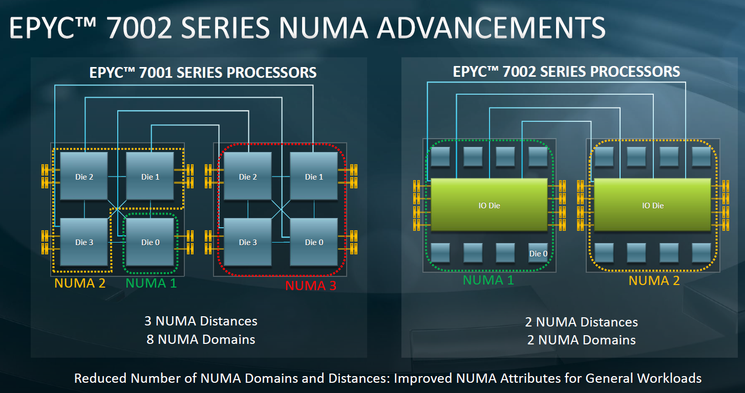
Just a Quick Question, all of the Epyc Rome systems are UMA right? Except fort he 2P system(two socket)? someone mentioned that all but the 64 core Rome Epycs were UMA(Uniform Memory Access)
 

DrMrLordX

Lifer
Apr 27, 2000
21,629
10,841
136
All Rome chips should be UMA within a single socket, including the 64c chips. There's one memory controller to rule them all, and on the substrate bind them.

Unless 64c EPYC has two I/O dice. I don't think it does.
 

naukkis

Senior member
Jun 5, 2002
706
578
136
All Rome chips can also configured to 4 numa socket per chip, 2 chiplets have a quarter of IO die and two memory channels. Memory latency will improve ~25ns and memory throughput some 10%, but with additional hassle with more numa nodes. Such a configuration option also tells that Rome IO chips is practically 4 Ryzen IO-chips linked together.
 
  • Like
Reactions: lightmanek

StefanR5R

Elite Member
Dec 10, 2016
5,509
7,816
136
All Rome chips should be UMA within a single socket, including the 64c chips. There's one memory controller to rule them all, and on the substrate bind them.
There are actually four 2-channel memory controllers in the IOD. Different CCDs experience slightly different latencies in memory accesses behind each of the four controllers.

Unless 64c EPYC has two I/O dice. I don't think it does.
All Epyc 7002 have just one IOD. (Putting two into one wouldn't bring any benefit without changing the socket also.)

All Rome chips can also configured to 4 numa socket per chip, 2 chiplets have a quarter of IO die and two memory channels. Memory latency will improve ~25ns and memory throughput some 10%, but with additional hassle with more numa nodes.
Indeed. Though on one hand, in many usage scenarios the higher count of NUMA nodes in the system is not a problem; on the other hand, the slightly decreased memory performance in the default UMA configuration is of negligible effect in most common workloads.

Such a configuration option also tells that Rome IO chips is practically 4 Ryzen IO-chips linked together.
Perhaps, but the actual implementation could be a bit more complex than that.
 
  • Like
Reactions: lobz and lightmanek

nicalandia

Diamond Member
Jan 10, 2019
3,330
5,281
136
All Rome chips can also configured to 4 numa socket per chip, 2 chiplets have a quarter of IO die and two memory channels. Memory latency will improve ~25ns and memory throughput some 10%, but with additional hassle with more numa nodes. Such a configuration option also tells that Rome IO chips is practically 4 Ryzen IO-chips linked together.

One Fat IO Chiplet to rule them all indeed.

Do you know if the new chipset for TR4 will use a Mirror Copy of the IO Chip like the X570 does for AM4? No news on new SP3 chipsets yet?
 

naukkis

Senior member
Jun 5, 2002
706
578
136
One Fat IO Chiplet to rule them all indeed.

Do you know if the new chipset for TR4 will use a Mirror Copy of the IO Chip like the X570 does for AM4? No news on new SP3 chipsets yet?

Actually x570 is interesting as AMD did not give details what it actually is. It's said to be Ryzen IO chip but build 14nm instead of 12nm. So did AMD plan to produce Ryzen IO-chip with 14nm and did do respin to 12nm and used already established 14nm lines to produce x570, or is x570 piece of Rome's IO chip? Because it's plain obvious that they won't establish own fab assembly for x570 when they could have used already in production 12nm IO-chip.

Which leads to what Threadripper IO-chip will be. Produced with 12nm it could provide higher memory clocks which are beneficial, but for economy reasons they would want to recycle Rome IO-chip.
 

DrMrLordX

Lifer
Apr 27, 2000
21,629
10,841
136
There are actually four 2-channel memory controllers in the IOD. Different CCDs experience slightly different latencies in memory accesses behind each of the four controllers.

Oh okay, thought it was one 8-channel controller. Which means . . .

Indeed. Though on one hand, in many usage scenarios the higher count of NUMA nodes in the system is not a problem; on the other hand, the slightly decreased memory performance in the default UMA configuration is of negligible effect in most common workloads.

Huh, didn't know you could force NUMA instead of UMA. That's kinda weird.
 

nicalandia

Diamond Member
Jan 10, 2019
3,330
5,281
136
Actually x570 is interesting as AMD did not give details what it actually is. It's said to be Ryzen IO chip but build 14nm instead of 12nm. So did AMD plan to produce Ryzen IO-chip with 14nm and did do respin to 12nm and used already established 14nm lines to produce x570, or is x570 piece of Rome's IO chip? Because it's plain obvious that they won't establish own fab assembly for x570 when they could have used already in production 12nm IO-chip.

Which leads to what Threadripper IO-chip will be. Produced with 12nm it could provide higher memory clocks which are beneficial, but for economy reasons they would want to recycle Rome IO-chip.

I was reading the the change to 12nm on Ryzen 3000 was to lower the power envelope as the AM4 platform is already constrained, but for TR4 and SP3 I don't believe that is the case. Both the 12nm and 14nm are built on GlobalFoundries
 

JoeRambo

Golden Member
Jun 13, 2013
1,814
2,105
136
Huh, didn't know you could force NUMA instead of UMA. That's kinda weird.

It is common technique in these big chips. Intel Skylake-SP also has this feature, where the die is split into two halves, each having access to half of memory controllers.
This mode has two benefits - one is obvious - for accessing die the latency is decreased, but also there is less load on internal interconnects on the other side of the die and that further helps with latencies and bandwidth.

The drawback is that workload needs to be NUMA aware ( or made into one with something like numactl ) AND fit in both NUMA memory ( half of what is connected to CPU in case of SKL-SP) and bandwidth ( also half ).
 
  • Like
Reactions: lightmanek

Markfw

Moderator Emeritus, Elite Member
May 16, 2002
25,551
14,510
136

Markfw

Moderator Emeritus, Elite Member
May 16, 2002
25,551
14,510
136
Might need to have an intervention. Put the wallet down sir!
I put myself on auto-notify for the 128 core 256 thread dual socket one..... I have the case and power supply required sitting idle. I just need memory I even have an extra nvme drive !
 
  • Like
Reactions: Drazick

nicalandia

Diamond Member
Jan 10, 2019
3,330
5,281
136
I put myself on auto-notify for the 128 core 256 thread dual socket one....
With this new design(Chiplets and Central IO) what would be the core limit per CPU of future Zen3/4/5(if they keep the 4ccx/8c chiplet)? For example if they get down to 5nm? according to this article: https://hothardware.com/news/tsmc-5nm-node-doubles-density-amd-ryzen-3000-7nm the density is nearly doubled, would that mean a 128 Core, 256 Threads single Socket Epyc CPU? 32 Core Mainstream CPU? Perhaps that would be restricted for Data Center CPUs as I can't even fathom such a massive CPU for mainstream
 

DarthKyrie

Golden Member
Jul 11, 2016
1,533
1,281
146
I put myself on auto-notify for the 128 core 256 thread dual socket one..... I have the case and power supply required sitting idle. I just need memory I even have an extra nvme drive !

I knew you wouldn't be able to pass that up.
 

DarthKyrie

Golden Member
Jul 11, 2016
1,533
1,281
146
With this new design(Chiplets and Central IO) what would be the core limit per CPU of future Zen3/4/5(if they keep the 4ccx/8c chiplet)? For example if they get down to 5nm? according to this article: https://hothardware.com/news/tsmc-5nm-node-doubles-density-amd-ryzen-3000-7nm the density is nearly doubled, would that mean a 128 Core, 256 Threads single Socket Epyc CPU? 32 Core Mainstream CPU? Perhaps that would be restricted for Data Center CPUs as I can't even fathom such a massive CPU for mainstream

It depends on how long it takes them to start doing the I/O on 7EUV instead of 14/12nm. I think that DDR memory stacking on the I/O die will come first.
 
  • Like
Reactions: lobz

Panino Manino

Senior member
Jan 28, 2017
821
1,022
136
All Rome chips should be UMA within a single socket, including the 64c chips. There's one memory controller to rule them all, and on the substrate bind them.

Unless 64c EPYC has two I/O dice. I don't think it does.

EPYC2NUMAadvantages.png
 

DarthKyrie

Golden Member
Jul 11, 2016
1,533
1,281
146
Actually due to the price, I may get 2 64 core threadrippers, I already have all the motherboard and coolers. Just want an option....

Has AMD confirmed that Zen2 TR will work in X399 or not? I haven't seen anything on the matter.
 

nicalandia

Diamond Member
Jan 10, 2019
3,330
5,281
136
It depends on how long it takes them to start doing the I/O on 7EUV instead of 14/12nm. I think that DDR memory stacking on the I/O die will come first.
I don't think they will be doing a 7nm IO chip at all since the reason for them not doing it along with the chiplet is that it will not scale linearly and very little gains will be obtain from 14/12nm process
 

DrMrLordX

Lifer
Apr 27, 2000
21,629
10,841
136
Only reason to move I/O die to any other process at the present or near future would be to finally cut off GF. 7nm would probably be suitable. Just more expensive.
 

DarthKyrie

Golden Member
Jul 11, 2016
1,533
1,281
146
I don't think they will be doing a 7nm IO chip at all since the reason for them not doing it along with the chiplet is that it will not scale linearly and very little gains will be obtain from 14/12nm process

The reasoning has to do with cost/benefit, once the cost of 7EUV comes down enough they will scale it down. AFAIK some of the stuff in the I/O die is present in their GPUs which means that those parts have been shrunk to 7nm already.