[Techpowerup] AMD "Zen" CPU Prototypes Tested, "Meet all Expectations"

Page 42 - Seeking answers? Join the AnandTech community: where nearly half-a-million members share solutions and discuss the latest tech.

Where do you think this will land performance wise

  • Intel i7 Haswell-E 8 CORE

  • Intel i7 Skylake

  • Intel i5 Skylake

  • Just another Bulldozer attempt


Results are only viewable after voting.

moonbogg

Lifer
Jan 8, 2011
10,635
3,095
136
In the last decade, I'd say Nehalem was the most important. Everything else has been building on that.

The first i7's were insanely exciting, especially because of that rumor that went around that said, "Core i7 won't be good at gaming". And then it came out and WRECKED THE EARTH at gaming and everything else.
However, the original i7's came at an odd time with regard to gaming. Dual core Wofldale's were still conquering the entire gaming landscape, and they were doing it at 4ghz quite commonly. Games that benefited from a quad core were very few and far between, if any existed at all and a great many gamers, including myself, simply skipped the entire first gen i7's, including their shrunken Westmere brethren because a fast dual core really was more than enough to wreck any game out there.
The release of BF Bad Company 2 would be the cold ice water on the backs of us dual core holdouts, forcing us to lock eyes with the amazing Sandy Bridge that was coming just around the corner.
 

myocardia

Diamond Member
Jun 21, 2003
9,291
30
91
Page table walks.

Which are pretty much irrelevant these days with Page Walk Caches in the MMU. PWCs allow for page table skipping.

Thank you. I've been amateurishly following CPUs since 1980, when I got my first one, but didn't ever remember hearing that term or acronym before. I'll file that away for future Cliff Claven monologues.:)

They're most certainly not irrelevant as they are a longer running process critical for calculating a memory address not found in the TLB/PWC/MMU cache. Often the caches reduce how much of the table you need to walk rather than eliminating walks entirely, so being able to have twice as many walks in flight at once is still beneficial.

The page table is an in-memory tree, after-all, so a cache hit lets you jump over a level or two and get to a closer branch to the address translation you need with much fewer memory accesses.

Still, it's probably only worth up to about 10~15% extra performance for the applications which see frequent TLB misses (large databases and games, for example), but it could be much more useful for SMT. If AMD gives both threads equal resource access in their SMT implementation, this could be a very big enabler for SMT scaling.

Thank you, that's awesome information. I'm imagining it also helping a company's CPU which has a somewhat slower cache as well.
 

myocardia

Diamond Member
Jun 21, 2003
9,291
30
91
The demand put on the MMU varies greatly depending on software -- a lot of well-behaved apps can live entirely out of tiny MMU caches, while other software can trash every level of every cache even if the caches are made huge. I've heard that large business apps written in Java or C# can spend a huge portion of their runtime in the page walker.

It's all starting to make sense now. More excellent info. Thanks.
 

Fjodor2001

Diamond Member
Feb 6, 2010
3,773
242
106
New info about the AMD Zen APU:

http://wccftech.com/amd-zen-hbm-apu-spotted/

AMD Zen APU Featuring HBM Spotted – 128GB/S Of Memory Bandwidth And Large On-Board GPU

An AMD Zen based APU featuring stacked High Bandwidth Memory – HBM – with 128GB/s of bandwidth and a large on-board GPU has been spotted. This came to light via a paper co-authored by one of AMD’s highest ranking graphics engineers, Mike Mantor.
[...]

AMD Zen APU Featuring HBM Spotted – 128GB/S Of Memory Bandwidth And Larger On-Board GPU Than Before

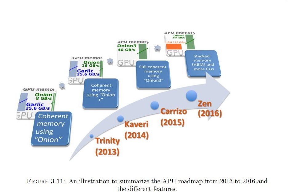
This latest paper is very interesting for a couple of reasons, the first is because it carries a very intriguing illustration that depicts a Zen APU featuring a next generation fully memory coherent interocnnect, dubbed Onion3 capable of 50GB/S of total bandwidth. This chip fabric is based on the evolution of the AMD coherent memory technology in Carrizo which is in itself is an improved design of the Playstation 4 and XBOX ONE’s interconnects. The illustration also makes mention of “more CUs” referring to graphics compute units, which indicates that Zen APUs will feature larger and more capable on-board graphics engines than what we’ve seen before.

AMD-Zen-APU-With-HBM.jpg


Additionally, the Zen based APU is also shown featuring HBM memory with 128GB/S of bandwidth. Which is the amount of bandwidth a single 4-Hi stack of first generation HBM can deliver. And that’s surprising, considering that in 2016 second generation HBM is expected to come to market with Nvidia’s Pascal and AMD’s Arctic Islands graphics chips. What’s even more peculiar is that the compandy did not announce any Zen based APUs for 2016. Instead, at AMD’s Financial Analyst Day Zen based APUs and enterprise class products were said to be coming in 2017.
 

tential

Diamond Member
May 13, 2008
7,355
642
121
Weird info but with hbm the on board gpu could be useful.

I've always said amd can win the market with console level performance apus in laptops and small pcs for the casual gamer crew and back to school people who may not be able to take a console with them..
We'll see how it pans out as always with amd.
 

Dresdenboy

Golden Member
Jul 28, 2003
1,730
554
136
citavia.blog.de
HBM + GPU is good for HPC, too. HBM as LLC (maybe already with NVRAM) on an Opteron ("disruptive memory bandwidth") would be good for data center applications.

But that's standard stuff and has been presented and described in slides and papers for years.

The craziest thing seen so far in patents are two separate frontends (incl. fetch and maybe even L1 I$) combined with a single backend. It has been mentioned like it's not that important (2 paragraphs). So far I didn't find papers looking at such a concept, but maybe someone here knows about such concepts in research.
 

Shehriazad

Senior member
Nov 3, 2014
555
2
46
iiiiiif all the rumors were true...this would be a monster all-rounder chip. But then again...rumors.


Whenever I hear "industry source" or "possibly"...I lose interest now. I mean yea. A 16/32 Thread Zen APU with 32mb L3, 16GB HBM and Greenland iGPU would totally wreck anything that currently exists on the market...but...I almost have to doubt AMDs capabilities of actually being able to deliver such a monster.

Of course they've always tried to innovate that market and whatnot...but as always, it comes down to their financial situation...and a chip like that sounds almost unbelievable...especially considering with how little R&D funding it would have to be made.

If a chip like this actually comes out in Q4 2016 /Q1 2017...I'd be the first to jump on it...but if it doesn't...I won't be terribly surprised, either.
 

Fjodor2001

Diamond Member
Feb 6, 2010
3,773
242
106
A 16/32 Thread Zen APU with 32mb L3, 16GB HBM and Greenland iGPU would totally wreck anything that currently exists on the market...but...I almost have to doubt AMDs capabilities of actually being able to deliver such a monster.

Of course they've always tried to innovate that market and whatnot...but as always, it comes down to their financial situation...and a chip like that sounds almost unbelievable...especially considering with how little R&D funding it would have to be made.
Such a chip would not be targeted to the consumer market, but to the server market. The APUs for consumer market will likely be 4-8 cores + iGPU + HBM2. Still very nice, and the chips will be much cheaper.

Also, it does not take much more R&D money to make a huge chip with 16/32 core CPU + more GPU cores + huge HBM. You just need more instances of the same IP blocks that already have been developed. The cost lies in developing the CPU and GPU core IP blocks to begin with. And from the info AMD has communicated, they have already designed those. It's just the production that lies ahead.
 

mrmt

Diamond Member
Aug 18, 2012
3,974
0
76
Also, it does not take much more R&D money to make a huge chip with 16/32 core CPU + more GPU cores + huge HBM. You just need more instances of the same IP blocks that already have been developed. The cost lies in developing the CPU and GPU core IP blocks to begin with. And from the info AMD has communicated, they have already designed those. It's just the production that lies ahead.

You have no idea on how such a design would stress the interconnects. CPUs cores are not GPU cores and have far different requirements for core count scaling. Core scaling is one of the features that I expect will make Zen flop on the server market.
 
Mar 10, 2006
11,715
2,012
126
You have no idea on how such a design would stress the interconnects. CPUs cores are not GPU cores and have far different requirements for core count scaling. Core scaling is one of the features that I expect will make Zen flop on the server market.

Rumor is that AMD will be using an MCM to get to higher core counts. If so, I would expect fairly poor multi-core scaling compared to the top Intel solutions in servers.
 

mrmt

Diamond Member
Aug 18, 2012
3,974
0
76
Sandy was way more important than Nehalem since Nehalem was still on the old Core architecture.

Nope, not at all. Nehalen marked the departure of the old FSB from Intel server infrastructure and the debut of QPI. It also marked the debut of the E7 series processors with Beckton, which initiated the implosion of IBM power business and dealt a huge blow on SUN's SPARC business, this on top of the excellent performance that the chip brought to the market. Those were far more important changes than anything Sandy Bridge brought to the market.

Don't get me wrong, Sandy Bridge on servers was a great product. It mopped the floor with AMD opterons line up and pushed x86 2P servers to until then unattainable levels of performance, even hitting some POWER and SPARC business with it, but it was built upon Nehalen's foundations.

I think the only comparable change in terms of magnitude will come with the Purley platform, where Intel will try different memory, interconnect and core IP for their server processors.
 
Last edited:
Mar 10, 2006
11,715
2,012
126
Nope, not at all. Nehalen marked the departure of the old FSB from Intel server infrastructure and the debut of QPI. It also marked the debut of the E7 series processors with Beckton, which initiated the implosion of IBM power business and dealt a huge blow on SUN's SPARC business, this on top of the excellent performance that the chip brought to the market. Those were far more important change than anything Sandy Bridge brought to the market.

Don't get me wrong, Sandy Bridge on servers was a great product. It mopped the floor with AMD opterons line up and pushed x86 2P servers to until then unattainable levels of performance, even hitting some POWER and SPARC business with it, but it was built upon Nehalen's foundations.

I think the only comparable change in terms of magnitude will come with the Purley platform, where Intel will try different memory, interconnect and core IP for their server processors.

100% agree. Great post, mrmt.
 

mrmt

Diamond Member
Aug 18, 2012
3,974
0
76
Rumor is that AMD will be using an MCM to get to higher core counts. If so, I would expect fairly poor multi-core scaling compared to the top Intel solutions in servers.

That would be too dumb even for AMD standards. That would confine them basically to the bottom of the server market.
 

Fjodor2001

Diamond Member
Feb 6, 2010
3,773
242
106
You have no idea on how such a design would stress the interconnects. CPUs cores are not GPU cores and have far different requirements for core count scaling. Core scaling is one of the features that I expect will make Zen flop on the server market.
Of course the interconnect requirements differ depending on core count. But interconnects is not what consumes most of the R&D budget. Design of CPU and GPU cores consume a much larger part of the total R&D costs.
 
Mar 10, 2006
11,715
2,012
126
Of course the interconnect requirements differ depending on core count. But interconnects is not what consumes most of the R&D budget. Design of CPU and GPU cores consume a much larger part of the total R&D costs.

Interconnect is a huge deal and very tricky to get right.
 

Fjodor2001

Diamond Member
Feb 6, 2010
3,773
242
106
There's lots of stuff that is tricky. But still, interconnects do not consume at all as big part of the R&D as CPU and GPU cores.
 

mrmt

Diamond Member
Aug 18, 2012
3,974
0
76
Of course the interconnect requirements differ depending on core count. But interconnects is not what consumes most of the R&D budget. Design of CPU and GPU cores consume a much larger part of the total R&D costs.

The interconnect is a very tricky decision because you cannot change it every single generation in a whim and it impacts the entire platform for generations to come, not only the chip you are designing. QPI for example will be 9 years old by the time of its retirement, and Intel had FSB for another 13 years.

So if you think AMD can "easily" escalate from 4 to 32 cores just because of validated IP you ought to have a surprise as soon as they release this line up, because either core scaling on the high core SKUs will be very, very poor (cheap is as cheap does) or the 4 core version will be saddled by expensive platform costs.

And the interconnect R&D cost is growing, not shrinking.
 
Last edited:

Dresdenboy

Golden Member
Jul 28, 2003
1,730
554
136
citavia.blog.de
Sandy was way more important than Nehalem since Nehalem was still on the old Core architecture.
This core heritage goes back to the P6. Since Banias the basic core layout (with a bit shuffling) didn't change dramatically. Well, even the PIII shows roughly the same layout. It's FP/SIMD units sit in one corner, the RS below, I$ diagonally located from FP/SIMD, D$ on the same row. It depends on orientation and mirroring, but after normalizing for this, it fits. When the smaller L2 reentered the rectangular core area, it did that on the D$ side, while it was on the I$ side in PIII.
PIII:


On that Hungarian site you can also find the architectural evolution from P6 to Skylake:
http://prohardver.hu/teszt/intel_architekturak_nehalemtol_skylake-ig/nyomtatobarat/teljes.html
(print view, easier to watch and scoll)
 
Last edited:

Fjodor2001

Diamond Member
Feb 6, 2010
3,773
242
106
@mrmt: I'm not saying it aint tricky. I'm just saying it consumes less R&D resources than CPU and GPU cores.

Also, didn't you read my previous post where I said interconnect requirements differ depending on core count?
 

Dresdenboy

Golden Member
Jul 28, 2003
1,730
554
136
citavia.blog.de
If a chip like this actually comes out in Q4 2016 /Q1 2017...I'd be the first to jump on it...but if it doesn't...I won't be terribly surprised, either.
An APU part in this timeframe is very unlikely.

The interconnect is a very tricky decision because you cannot change it every single generation in a whim and it impacts the entire platform for generations to come, not only the chip you are designing. QPI for example will be 9 years old by the time of its retirement, and Intel had FSB for another 13 years.

So if you think AMD can "easily" escalate from 4 to 32 cores just because of validated IP you ought to have a surprise as soon as they release this line up, because either core scaling on the high core SKUs will be very, very poor (cheap is as cheap does) or the 4 core version will be saddled by expensive platform costs.

And the interconnect R&D cost is growing, not shrinking.
And is it growing from $1M to $10M or from $100M to $1B?

And why do you mix external interconnects with intra die communication (XBar, ring bus, other busses, etc)?
 

dark zero

Platinum Member
Jun 2, 2015
2,655
138
106
Rumor is that AMD will be using an MCM to get to higher core counts. If so, I would expect fairly poor multi-core scaling compared to the top Intel solutions in servers.
In the best case AMD will get Power tier levels.... with only 2 threads... so they must think about lower prices or using nVILINK since Intel won't likely allow to use it on their machines....
 

mrmt

Diamond Member
Aug 18, 2012
3,974
0
76
An APU part in this timeframe is very unlikely.


And is it growing from $1M to $10M or from $100M to $1B?

And why do you mix external interconnects with intra die communication (XBar, ring bus, other busses, etc)?

Certainly not from 1M to 10M, unless we are talking about that primitive AMD crossbar.

And I do mix the two because in the server world they are part of the same problem: You need to reach a certain level of performance and for that you need a certain number of cores, whether you'll have these cores in 1, 2 or 4 dies is irrelevant as long as TCO is fine.