Speculation: Ryzen 4000 series/Zen 3

Page 85 - Seeking answers? Join the AnandTech community: where nearly half-a-million members share solutions and discuss the latest tech.

eek2121

Platinum Member
Aug 2, 2005
2,930
4,026
136
Mmmmm....
I also have been following the USPTO website closely. But I am not sure how he discovers those are going to make it to Zen 3

I expect most of those patents won't apply to Zen 3. I imagine Zen 3 will bring improved clocks, FPU performance (possibly with AVX-512), and higher IPC. Although the family change from 17h to 19h does intrigue me...

I imagine any game changing stuff will land with Zen 4.

I kind of wish AMD would roll out AM5 this year and either make the CPUs interchangable or make AM4 and AM5 versions of Zen 4000. Absent that, I wish they would commit to AM4 for a couple more years. As a Zen 1 Threadripper 1950X user, they have left me in an odd position. It seems that if I upgrade now, I will will have to buy another motherboard, only to have to buy another motherboard again for my next upgrade after that. I needed 16 cores, but I have no desire to upgrade to TRX40, as the 3950X would likely satisfy my workloads.

That being said, I am fine with riding things out until AM5 if need be.
 

eek2121

Platinum Member
Aug 2, 2005
2,930
4,026
136
Courtesy of Hexus

AMD Ryzen 7 4800HS appears in Time Spy CPU benchmarks

An encouraging benchmark run for the AMD Ryzen 7 4800HS APU has been unearthed in the 3DMark Time Spy benchmark online results browser. First of all you might be asking what is the Ryzen 7 4800HS? At the launch of the Ryzen 4000 Series mobile APUs AMD revealed details about the Ryzen 7 4800H, and this 4800HS model appears to be an optimised top-binned 35W version of that mobile APU, destined for premium gaming laptops.


d522a424-8eb6-4bfe-ae7b-e224671846e7.jpg


Twitter's Tum Apisak found the AMD Ryzen 7 4800HS in Time Spy benchmarks online and has listed its CPU score alongside friends and rivals as below:
Time Spy CPU Score
  • R7 4800HS - 8,730
  • R7 4800H - 8,350
  • R7 3700X - 10,180
  • R7 2700X - 8,600
  • R5 3600 - 7,300
  • R5 3600 - 7,150
  • i7-9700K - 8,200
24d1419c-5be0-4e90-afea-355bca4dfe1b.jpg


The above table is all the more remarkable when one considers the TDPs of the chips that are listed. The AMD Ryzen 7 4800HS is a 35W part, the standard 4800H a 45W part. Compared to a previous gen desktop part, the powerful 105W AMD Ryzen 7 2700X, the new 4800HS still comes ahead in this CPU score benchmark run. All the aforementioned CPUs have a 8C/16T configuration. The sole Intel entry in the comparison list above is the 8C/8T Core i7-9700K, which has a 95W TDP and a Time Spy CPU Score of 8,200.

d29acf70-a401-4aaf-8f7e-2887d4ee0d80.jpg


Time Spy CPU Scores that leak out like this might have a lot of variance due to other system components and so on, however, it is still a tantalising indicator that there are some exceedingly beefy AMD powered laptops on the way.
Lenovo touts AMD Ryzen 9 4900U powered laptops
On the topic of AMD 4000 series mobile APUs, Lenovo was recently spotted showing off its latest Yoga Slim 7 family of 2-in-1 laptops with choice of AMD or Intel processors. Notebook Italia recorded a video of the exhibition which claimed one of the laptops came with an AMD Ryzen 9 4900U inside.

The source has since blurred out the AMD processor info in the video(embedded above), saying it was a typo on the Lenovo specs list. It is hard to be sure if this is the case, or if AMD exerted some pressure on its partners to keep the Ryzen 9 4900XX APUs under wraps for now. Interestingly the official Yoga Slim 7 (14-inch, AMD) product page still lists the processor as an AMD Ryzen 4000 Series, with choice of "up to AMD Ryzen 9," available for users to configure.

This reminds me: I wouldn't be surprised if AMD does away with chiplets and goes back to a monolithic die. They are working with what is now a very mature process, and they can easily bin chips based on silicon quality (as mobile is demonstrating).
 

soresu

Platinum Member
Dec 19, 2014
2,657
1,858
136
This reminds me: I wouldn't be surprised if AMD does away with chiplets and goes back to a monolithic die. They are working with what is now a very mature process, and they can easily bin chips based on silicon quality (as mobile is demonstrating).
It's not just about yield, it's about the design itself, which is very expensive - GPU's tend to be a bit simpler, but not enough to drastically counter the increase in spending on the silicon design process (ie all the masks and whatnot that come before the initial tape out stage).

Apparently this has shot way up for 7nm, and 5nm+ will only get worse - I don't know if EUV will reduce the complexity of this for them much or at all.

Chiplets also allow them to tune each portion of the chip to a specific process for max performance/power, AMD have said before that having the APU on one process is not ideal as CPU and GPU can perform better if tuned separately - I can't remember the exact words they used, it could have been as far back as Carrizo or Kaveri.
 

amrnuke

Golden Member
Apr 24, 2019
1,181
1,772
136
I expect most of those patents won't apply to Zen 3. I imagine Zen 3 will bring improved clocks, FPU performance (possibly with AVX-512), and higher IPC. Although the family change from 17h to 19h does intrigue me...

I imagine any game changing stuff will land with Zen 4.

I kind of wish AMD would roll out AM5 this year and either make the CPUs interchangable or make AM4 and AM5 versions of Zen 4000. Absent that, I wish they would commit to AM4 for a couple more years. As a Zen 1 Threadripper 1950X user, they have left me in an odd position. It seems that if I upgrade now, I will will have to buy another motherboard, only to have to buy another motherboard again for my next upgrade after that. I needed 16 cores, but I have no desire to upgrade to TRX40, as the 3950X would likely satisfy my workloads.

That being said, I am fine with riding things out until AM5 if need be.
If Zen3 has AVX-512 that will be a killer. I doubt it, but if it does... there will be little reason left to go with Intel for anything outside of 1080p144-240 gaming.
 

itsmydamnation

Platinum Member
Feb 6, 2011
2,765
3,131
136
If Zen3 has AVX-512 that will be a killer. I doubt it, but if it does... there will be little reason left to go with Intel for anything outside of 1080p144-240 gaming.
i dont think we will see 512bit data paths , but we could see avx-512 supported. The rumor was 4x 256bit FMA, if it also supported AVX512 over 2 cycles then you get the newer instructions along with awesome thoughtput for the more used smaller vectors.
 

jamescox

Senior member
Nov 11, 2009
637
1,103
136
This reminds me: I wouldn't be surprised if AMD does away with chiplets and goes back to a monolithic die. They are working with what is now a very mature process, and they can easily bin chips based on silicon quality (as mobile is demonstrating).

You can get a desktop apu with 8 cores. Anything else will almost certainly still be chiplet based. They can’t do larger parts as a monolithic die and there is a lot of reasons not to. Intel’s 28 core is around 700 square mm. Two of them to be remotely competitive with with EPYC is around 1400 square mm and a lot more expensive than 8 tiny 75 mm square chips on 7 nm and a large IO die on an old process. I believe EPYC is over 1000 mm square total.

Even the smaller chips are going to be a lot cheaper to make as a combination of 14 nm io die and cpu chiplets. For the 16 core, that would be 150 square mm just for the cpu cores possibly around 100 for io die (doesn’t scale well with shrink, so probably at least 80). That would be a big die for 7 or 5 nm yields. They wouldn’t be able to have such large caches with a monolithic die. For the chiplet based design, they can sell anything with 2, 3, or 4 good cores per CCX. With a monolithic die, there is a lot less options. A defect in the io portion of a monolithic die could make the entire die unusable. Yields are still a big part of the reason for chiplets. The larger core count parts would be astronomically expensive to make as a monolithic die and anything bigger than the reticule, over 800 square mm, isn’t really manufacturable.

Zen 3 will be moving to an 8 core CCX with 32 MB L3 cache. That is actually the same amounts as current zen 2, just connected differently. That will remove one of the few places where intel does better than AMD due to high end Xeons having up to 37.5 MB of cache accessible to a single core.

The “Intel is better for gaming” is just BS. Running at low resolution and low quality is really just a fancy memory latency test. It isn’t really indicative of real world performance. Anyway, a lot more things will be cacheable with 32 MB L3 and probably a bunch of other cache improvements, including better prefetch. The whole idea of caching is to hit the memory latency as infrequently as possible. If they implement significantly improved AVX2 throughput, Then there may not really be much of anything where intel wins, even if they don’t implement avx512.
 

jamescox

Senior member
Nov 11, 2009
637
1,103
136
AMD verbiage particularly Forst Norrods has been the exact opposite. Zen2 was a more "minor"update and Zen3 is a bigger update. I dont trust any of the rumors but what we have so far is:

8 Core CCX ( amd presentation)
big (50%) L1 bandwidth increase (rumor)
4x 256 FMA (rumor)
big FPU performance incerease (rumor)
3d stacking of SRAM ( few rumors , new patients)

We haven't heard any rumors on the front-end/INT core but even if you just assume only evolutionary changes, that still better /bigger branch/fetch/predict/retire/PRF etc .

assuming all are true holistically that a very big uplift in the Core to memory sub system/a cache design. The requirements of the IF/cache coherency will change massively if AMD stack stacking 100's/1000's of MB of SRAM on each CCD.

There isn’t going to be “100’s/1000’s of MB of SRAM on each CCD”. SRAM isn’t that dense. The 32 MB of L3 cache on Zen 2 die probably takes up about 45% of the die, about 45% for cores, and about 10% for infinity fabric. That is just guessing based on die photos. With a stacked L3 cache die they may be able to fit 16 cores on the logic die and 64 MB on the cache chip. They could fit more at 5 nm though, so with larger die, maybe 128 MB of L3, since it scales so well with process shrinks. They also may do better with a die optimized specifically for cache. I don’t think this is a zen 3 thing though; probably Zen 4 or 5.

There isn’t going to be HBM either. HBM is still DRAM which is too high of latency for a cpu cache. Where caches are concerned, larger is slower since it takes longer to look up. I don’t really expect any stacked chips with Zen 3. I think it will be very similar at the package level. Eight cpu cores and 32 MB of L3 cache per CCD is actually the same as Zen 2, it is just in 1 CCX in zen 3 instead of 2 in Zen2. The 32 MB L3 will probably be slightly slower, so they may increase L2 cache size to make up for it. The die size may still be similar, even with more L2, due to 7nm+.

With zen 3 being a new family, I would expect a lot of the other improvements to be there. If they are doing a completely new floor plan, I would expect a lot of drastic changes. Going up to 4 full function AVX256 units isn’t really that drastic. Making 2 AVX 2 units support AVX512 or support for AVX512 across two clocks would be a bit more drastic, but it isn’t really new either since that is how they handled AVX 2 with 128-bit units previously. Adding new AVX512 instructions would be a bit of work though. Improved FP is a certainty and it does require a lot of increased throughput, so I would expect cache throughput has all been upgraded also, we just don’t really know how much it has been improved.

One outlier possibility is that they support stacking an extra cache chip on top, possibly as L4, but only for high end HPC or database processors and such. That my be worthwhile for such expensive parts, but for anything else, it isn’t really. I still don’t think it would be a Zen 3 feature, but that could explain the larger than 32 MB rumors. They could also just make a larger L3 die variant with Zen3.
 
  • Like
Reactions: Gideon

jpiniero

Lifer
Oct 1, 2010
14,585
5,209
136
The “Intel is better for gaming” is just BS.

It's a per core performance test really. More cores, better SMT yield, etc, isn't going to help. Better IPC and more frequency does. Memory speed/latency does help in some cases.

Now... you might need a fast, expensive GPU to make a real difference.
 

lobz

Platinum Member
Feb 10, 2017
2,057
2,856
136
It's a per core performance test really. More cores, better SMT yield, etc, isn't going to help. Better IPC and more frequency does. Memory speed/latency does help in some cases.
IPC is at least on par for both CPU vendors and average frame rates vary by some percents, while
...you (might) need a fast, expensive GPU to make a real difference.
Exactly.
 
  • Like
Reactions: trollspotter

Olikan

Platinum Member
Sep 23, 2011
2,023
275
126
Apparently this has shot way up for 7nm, and 5nm+ will only get worse - I don't know if EUV will reduce the complexity of this for them much or at all.

It will actually be better, a nice reduction to mask count (similar number of N16), reductions of double, quad patterning to single pass... yields and parametrics yields, should be way better

While less complex, there are other issues, masks are way more expensive. And production up time is worse...
 

eek2121

Platinum Member
Aug 2, 2005
2,930
4,026
136
Just a few points of clarification: To my knowledge, AMD has never stated they are moving to an 8 core CCX, only that the L3 cache would not be split.

In regards to chiplets vs. monolithic design, both have pros and cons, but most here don't understand why AMD went the chiplet route in the first place, and why chiplets don't matter now.

At the time AMD planned to move to 7nm, yields were low, machine time was expensive, and Fab capacity was low. By creating 8 core chiplets, AMD could easily harvest the most dies possible and also keep machine times down. By utilizing the already 14/12nm process for IO dies, AMD was able to use more of the wafer for the actual CPU cores. This allowed them to produce more product in less time. It actually had little to do with binning, and everything to do with cost.

With yields of both 7nm and 7nm EUV being 90+%, and Fab capacity being much higher, there is little sense to continue the chiplet design as packaging costs are higher, latency is higher, and there are other ways to bin.

The one exception to this would be if 7nm EUV capacity is constrained and they need to utilize 7nm (non EUV) or 12/14nm for parts of the chip, or they are developing a unique type of design that is easier done with chiplets.
 

itsmydamnation

Platinum Member
Feb 6, 2011
2,765
3,131
136
There isn’t going to be “100’s/1000’s of MB of SRAM on each CCD”. SRAM isn’t that dense. The 32 MB of L3 cache on Zen 2 die probably takes up about 45% of the die, about 45% for cores, and about 10% for infinity fabric. That is just guessing based on die photos. With a stacked L3 cache die they may be able to fit 16 cores on the logic die and 64 MB on the cache chip. They could fit more at 5 nm though, so with larger die, maybe 128 MB of L3, since it scales so well with process shrinks. They also may do better with a die optimized specifically for cache. I don’t think this is a zen 3 thing though; probably Zen 4 or 5.

One outlier possibility is that they support stacking an extra cache chip on top, possibly as L4, but only for high end HPC or database processors and such. That my be worthwhile for such expensive parts, but for anything else, it isn’t really. I still don’t think it would be a Zen 3 feature, but that could explain the larger than 32 MB rumors. They could also just make a larger L3 die variant with Zen3.
Remember its TSV and the patients talk about how they handle dummy dies for parts of the die that aren't stacked. The end result is that you could have high's 100's because you can stack as many dies as you want, we currently do upto 12 for dram. They could also run denser lower clocking sram or the other option is edram. I imaging what AMD would do for stacked memory chips is that for consumer chips the regular L3 acts as a regular L3 and there is no die stacking. high clocks would still favour 2d chips anyway. For server and other parts N number of *ram dies are used and X percentage of the L3 is used to hold tag/directory info for the cache lines in the stacked dies, the more stacks the more percentage of L3 is used. This would be much like HT assist or even the L2 shadow tags that AMD use now.


There isn’t going to be HBM either. HBM is still DRAM which is too high of latency for a cpu cache. Where caches are concerned, larger is slower since it takes longer to look up. I don’t really expect any stacked chips with Zen 3. I think it will be very similar at the package level. Eight cpu cores and 32 MB of L3 cache per CCD is actually the same as Zen 2, it is just in 1 CCX in zen 3 instead of 2 in Zen2. The 32 MB L3 will probably be slightly slower, so they may increase L2 cache size to make up for it. The die size may still be similar, even with more L2, due to 7nm+.

Yes HBM can be used as a bandwidth amplifier but offers no latency improvements, So there could still be workloads it is worthwhile using.
I wouldn't be surprised either way in terms of die stacking being available or not , the thing to consider is that if there are big Jumps in FPU throughput the socket is still limited to 8 channel DDR and memory bandwidth will become a limiting factor.

With zen 3 being a new family, I would expect a lot of the other improvements to be there. If they are doing a completely new floor plan, I would expect a lot of drastic changes. Going up to 4 full function AVX256 units isn’t really that drastic. Making 2 AVX 2 units support AVX512 or support for AVX512 across two clocks would be a bit more drastic, but it isn’t really new either since that is how they handled AVX 2 with 128-bit units previously. Adding new AVX512 instructions would be a bit of work though. Improved FP is a certainty and it does require a lot of increased throughput, so I would expect cache throughput has all been upgraded also, we just don’t really know how much it has been improved.
4x 256bit FMA is a much bigger change then you give credit and would be much harder to implement then 2x512 FMA. Thats because you require significantly more read/write ports to the F-RPF and that is hard. I would expect AVX-512 with VNNI to be supported. If AMD does 512bit data paths and 512bit vector units all they have done is improve AVX-512. If AMD increase memory/L1D throughput by other means and makes all FPU ports add+mul/fma that will benefit far more workloads from the INT side to SSE to AVX-512. I really hope AMD takes the more general approach.
 
  • Like
Reactions: lightmanek

itsmydamnation

Platinum Member
Feb 6, 2011
2,765
3,131
136
In regards to chiplets vs. monolithic design, both have pros and cons, but most here don't understand why AMD went the chiplet route in the first place, and why chiplets don't matter now.


At the time AMD planned to move to 7nm, yields were low, machine time was expensive, and Fab capacity was low. By creating 8 core chiplets, AMD could easily harvest the most dies possible and also keep machine times down. By utilizing the already 14/12nm process for IO dies, AMD was able to use more of the wafer for the actual CPU cores. This allowed them to produce more product in less time. It actually had little to do with binning, and everything to do with cost.

With yields of both 7nm and 7nm EUV being 90+%, and Fab capacity being much higher, there is little sense to continue the chiplet design as packaging costs are higher, latency is higher, and there are other ways to bin.
fundamentally disagree with this, your ignoring that one CCD is used across 17 core configurations and 3 memory configurations you have just exploded the development cost to meet all those markets. Your also ignoring that chiplets allow amd to easily pass the rectile limits of a process which is normally around 500-600mm^2. Then when AMD moves to 5nm how do you expect to yield a 600-800mm^2 96-128 core monolithic processor?

When AMD starts die stacking do you want to throw away 500mm^2 of 7+/5/5+ and a large amount of stacked dies on one bad stack or only 70mm^2 IOD and a smaller amount of stacked die ?

Your reasoning of package cost isn't sound , we have been using simple flip chip MCM packaging for decades on even mass manufactured consumer goods like the wii or the xbox360.
 

maddie

Diamond Member
Jul 18, 2010
4,738
4,667
136
Just a few points of clarification: To my knowledge, AMD has never stated they are moving to an 8 core CCX, only that the L3 cache would not be split.

In regards to chiplets vs. monolithic design, both have pros and cons, but most here don't understand why AMD went the chiplet route in the first place, and why chiplets don't matter now.

At the time AMD planned to move to 7nm, yields were low, machine time was expensive, and Fab capacity was low. By creating 8 core chiplets, AMD could easily harvest the most dies possible and also keep machine times down. By utilizing the already 14/12nm process for IO dies, AMD was able to use more of the wafer for the actual CPU cores. This allowed them to produce more product in less time. It actually had little to do with binning, and everything to do with cost.

With yields of both 7nm and 7nm EUV being 90+%, and Fab capacity being much higher, there is little sense to continue the chiplet design as packaging costs are higher, latency is higher, and there are other ways to bin.

The one exception to this would be if 7nm EUV capacity is constrained and they need to utilize 7nm (non EUV) or 12/14nm for parts of the chip, or they are developing a unique type of design that is easier done with chiplets.
Stating yield as 90%+ makes me assume you need to do some more thinking on this. I can guarantee than a yield of 90% on a small die translates to much less yield on one 4-6 times the size as yield is dependent on defect density and area of the die. Stating 90% yield by itself tells us very little. Maybe you're thinking that defect density has dropped to very low levels. I suggest you do the math or use the online die yield calculators to see for yourself the benefits of smaller chiplets vs a comparable monolithic die.

In any case, I assume that AMD will be transitioning to new nodes ASAP and will always be looking at maximizing yields. In the race with Intel, they do not have the benefit to use a node for long periods. 14 nm with Intel was an anomaly. We upgraded process much faster in the past and seem to be returning to this reality. The older members will know this.
 
  • Like
Reactions: spursindonesia

moinmoin

Diamond Member
Jun 1, 2017
4,944
7,656
136
In any case, I assume that AMD will be transitioning to new nodes ASAP and will always be looking at maximizing yields. In the race with Intel, they do not have the benefit to use a node for long periods. 14 nm with Intel was an anomaly.
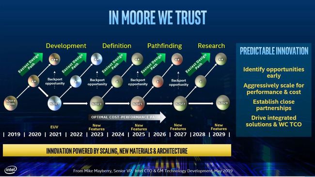
Indeed. As we all saw Intel already announced last May (leaked to public in December) they want to go back to realizing a new node every two years. This is what AMD has to plan to be prepared for.

23SidpbEDAxxLhEEwXks7J-650-80.jpg
 

eek2121

Platinum Member
Aug 2, 2005
2,930
4,026
136
TSMC themselves have stated that they have 90%+ yields for both 7nm and 7nm EUV.

I never stated they wouldn't eventually return to a chiplet based design, only that most don't understand why they did it in the first place.

Keep in mind that mobile isn't using chiplets. The next gen consoles don't appear to be using chiplets. It is even possible that EPYC and Threadripper could use a chiplet based design, but Ryzen could be monolithic.

I suspect AMD's current priorities are to increase clocks and obtain feature parity with Intel, improve IPC, reduce power consumption, and most of all, focus on higher margins. I also expect they are working on getting a GPU integrated with Ryzen desktop.

I doubt we'll see any form of "stacking" with Zen 3. I believe that is still in the development phases, there are many challenges to overcome.

Most of the big changes will land when AMD moves to a new socket.
 

maddie

Diamond Member
Jul 18, 2010
4,738
4,667
136
TSMC themselves have stated that they have 90%+ yields for both 7nm and 7nm EUV.

I never stated they wouldn't eventually return to a chiplet based design, only that most don't understand why they did it in the first place.

Keep in mind that mobile isn't using chiplets. The next gen consoles don't appear to be using chiplets. It is even possible that EPYC and Threadripper could use a chiplet based design, but Ryzen could be monolithic.

I suspect AMD's current priorities are to increase clocks and obtain feature parity with Intel, improve IPC, reduce power consumption, and most of all, focus on higher margins. I also expect they are working on getting a GPU integrated with Ryzen desktop.

I doubt we'll see any form of "stacking" with Zen 3. I believe that is still in the development phases, there are many challenges to overcome.

Most of the big changes will land when AMD moves to a new socket.
They can't use 90% yields in isolation. They must have related it to some sized die. For example, we are getting 90%+ yields on this 100mm^2 whatever. They won't just say no matter the size of your die, you'll get 90% yield.

Go and read the 1st generation Zen threads. I think most here understand why chiplets, and remember costs are a lot more than just fab costs. Inventory control, design, SKU flexibility, etc.

As regards to monolithic in mobile, one of the main drawbacks with chiplets is the constant fabric power consumption. This prevents a very low power state in the SOC, because if you try to go low power in the fabric, then you increase response time, a lot. With present tech, You can't wake quickly from low power states.

This is one reason why I believe mobile will stay monolithic for a long time.
 

Ajay

Lifer
Jan 8, 2001
15,431
7,849
136
Indeed. As we all saw Intel already announced last May (leaked to public in December) they want to go back to realizing a new node every two years. This is what AMD has to plan to be prepared for.

23SidpbEDAxxLhEEwXks7J-650-80.jpg
This is a pipe dream, IMO. I mean, it looks pretty- very orthogonal. Looks like something drawn up by marketing, not engineering (you’d think they’d learn from tick-tock). As feature size decreases, neat little patterns break down.
 

DrMrLordX

Lifer
Apr 27, 2000
21,620
10,830
136
Keep in mind that mobile isn't using chiplets. The next gen consoles don't appear to be using chiplets. It is even possible that EPYC and Threadripper could use a chiplet based design, but Ryzen could be monolithic.

I suspect AMD's current priorities are to increase clocks and obtain feature parity with Intel, improve IPC, reduce power consumption, and most of all, focus on higher margins. I also expect they are working on getting a GPU integrated with Ryzen desktop.

AMD has prioritized server CPU development. Desktop/workstation gets the scraps of that development, which is why desktop/workstation gets the same basic CPU topology as server. Mobile gets an entirely new design based on the same uarch/mem controller but on one die, since power demands are too different to accommodate parts designed for the server. The only way I see this changing is if AMD knocks desktop down a peg and just stops releasing desktop chips along the same cadence as Zen/Zen+/Zen2. Their current cadence is:

Feb/March : ODM shipments of server parts
July: Desktop launch of same gen
Aug/Sept: Public launch of server parts
Oct/Nov: Workstation launch of same gen
Dec/Jan: Mobile launch of same gen

The earliest they could change cadence would be Zen4. In which case we could see Genoa in Feb/March 2021 to ODMs (Aug/Sept for everyone else), Oct/Nov for Zen4 Threadripper and then Dec 2021 or Jan2022 for Zen4 desktop and mobile.
 

jamescox

Senior member
Nov 11, 2009
637
1,103
136
It's a per core performance test really. More cores, better SMT yield, etc, isn't going to help. Better IPC and more frequency does. Memory speed/latency does help in some cases.

Now... you might need a fast, expensive GPU to make a real difference.

What is the core actually doing when running at something like 200 FPS? It has to make a pass through the scene data, process some draw calls, and throw it at the gpu. That sounds a lot like it will be memory latency bound. The entire scene isn’t going to fit in cache. If it did fit in cache, then we could actually ray trace it at high speed.

Note that huge numbers of people use IPC without really understanding how it works. I have profiled some, seemingly compute bound task, only to find that they were actually achieving an IPC of around 1. IPC varies widely across applications and the average memory latency is a big part of what the actual achievable IPC is. You can’t define a core IPC independent of the memory system. Your IPC is zero while waiting on memory. AMD probably has better average latency in many cases due to the large caches (2*16 MB). If you put it in a contrived situation though, Intel does have better latency when actually going all of the way out to DRAM, so I am still of the opinion that these low quality/low res test with a powerful gpu are testing memory latency and probably not much else.
 

jamescox

Senior member
Nov 11, 2009
637
1,103
136
Remember its TSV and the patients talk about how they handle dummy dies for parts of the die that aren't stacked. The end result is that you could have high's 100's because you can stack as many dies as you want, we currently do upto 12 for dram. They could also run denser lower clocking sram or the other option is edram. I imaging what AMD would do for stacked memory chips is that for consumer chips the regular L3 acts as a regular L3 and there is no die stacking. high clocks would still favour 2d chips anyway. For server and other parts N number of *ram dies are used and X percentage of the L3 is used to hold tag/directory info for the cache lines in the stacked dies, the more stacks the more percentage of L3 is used. This would be much like HT assist or even the L2 shadow tags that AMD use now.


Yes HBM can be used as a bandwidth amplifier but offers no latency improvements, So there could still be workloads it is worthwhile using.
I wouldn't be surprised either way in terms of die stacking being available or not , the thing to consider is that if there are big Jumps in FPU throughput the socket is still limited to 8 channel DDR and memory bandwidth will become a limiting factor.


4x 256bit FMA is a much bigger change then you give credit and would be much harder to implement then 2x512 FMA. Thats because you require significantly more read/write ports to the F-RPF and that is hard. I would expect AVX-512 with VNNI to be supported. If AMD does 512bit data paths and 512bit vector units all they have done is improve AVX-512. If AMD increase memory/L1D throughput by other means and makes all FPU ports add+mul/fma that will benefit far more workloads from the INT side to SSE to AVX-512. I really hope AMD takes the more general approach.

You can stack huge amounts of DRAM and huge amounts of flash die since they take very little power when not being accessed and very little of it is ever accessed at one time. With flash drives, the heatsink is generally for the controller, not really the actual memory die. That isn’t the case with SRAM. It takes a lot of power even when not being actively accessed and is accessed much more frequently, so you are not going to see huge stacks of it. You also have a cpu some where in the stack which is also going to push the stack power limits.

The other reason that you aren’t going to see such large caches is that bigger is slower. Going up to such large sizes would quickly fail as L3 cache due to the reduced speed. Going from 8->16 between Zen1 and Zen2 increased access latency a bit, and that would get much worse at larger sizes. Using EDRAM would be very slow for a processor cache. You would be already starting at very high access times due to large size and add on DRAM cell read latency. Since they don’t want to slow down L3 cache significantly, most likely path may be adding another level of cache hierarchy for applications that could use it; some HPC applications, large database applications, and such. It would be unnecessary for desktop parts, so they would probably be limited to on die L3 with no L4. Implementing it as a large, stacked L3 would probably not be good. The size wouldn’t make up for the access latency. They may need to increase L2 size just to make up for access latency to 32 MB cache. If you start talking about 64, 128, or even more, then that pretty much can’t be L3 cache.

The memory bandwidth issues that seem to always be brought up just don’t seem to have materialized. The Threadripper 3990x seems to be doing quite well with just 4 channels. Large, fast caches and good prefetch seems to work very well. We have DDR5 coming eventually, so there could be some bandwidth bottlenecks with DDR4. I am okay with the floating point hardware being so powerful that it hits a bandwidth bottleneck.
 
Last edited:

RetroZombie

Senior member
Nov 5, 2019
464
386
96
They can't use 90% yields in isolation. They must have related it to some sized die. For example, we are getting 90%+ yields on this 100mm^2 whatever.
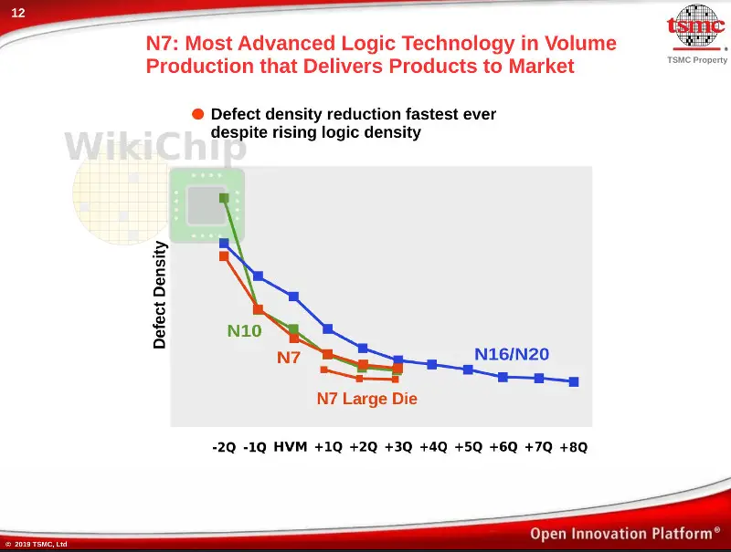
You are right but they strangely put out this slide where the big dies have even better yield (or less defects) than the small ones or i'm reading it incorrectly.

vlsi-2019-tsmc-n7-yield-2.jpg
 

jpiniero

Lifer
Oct 1, 2010
14,585
5,209
136
What is the core actually doing when running at something like 200 FPS? It has to make a pass through the scene data, process some draw calls, and throw it at the gpu. That sounds a lot like it will be memory latency bound. The entire scene isn’t going to fit in cache. If it did fit in cache, then we could actually ray trace it at high speed.

Compared to Matisse, it's more the all core frequency that's the difference.