Question Speculation: RDNA3 + CDNA2 Architectures Thread

uzzi38

Platinum Member
Oct 16, 2019
2,565
5,575
146

Det0x

Golden Member
Sep 11, 2014
1,027
2,953
136

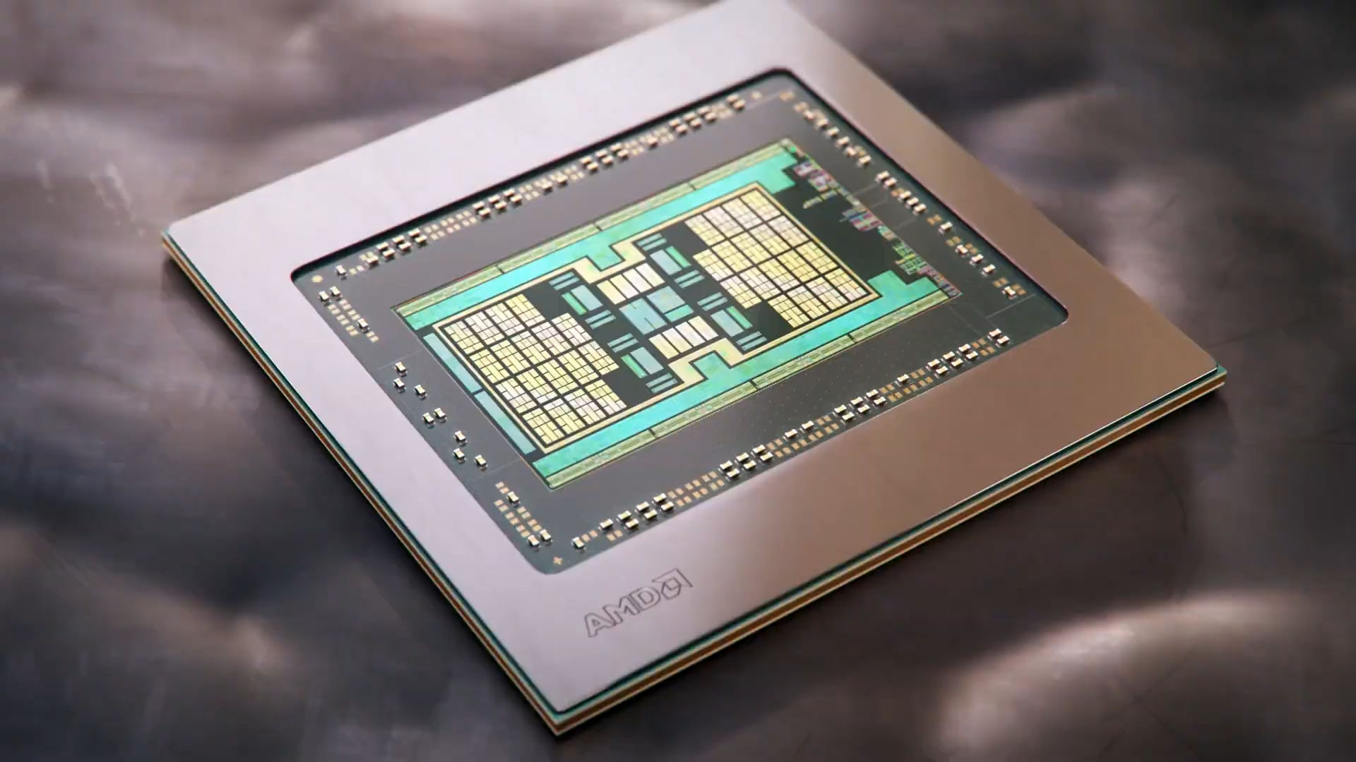
AMD Navi 31, the first desktop chiplet-based GPU?
Navi 31 shaping into a true compute monster.

We have heard rumors about the upcoming Navi 31 GPU for a while now. In fact, there have been rumors about Navi 41 already. The Navi 31 might be AMD’s first MCM (multi-chip module) design. NVIDIA is too expected to take the same route with its Hopper series, however, it remains unclear if the architecture is meant for gaming or compute workloads. On the other hand, AMD made it clear that RDNA3 has Radeon DNA and it is for sure aiming at the gaming market.

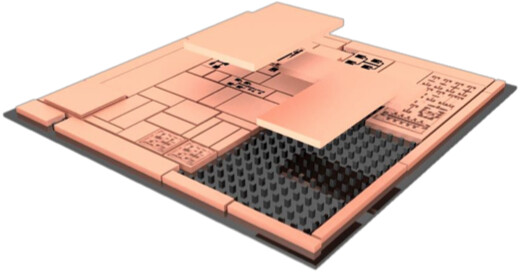
The successor to Instinct MI100 (no longer called Radeon) based on Arcturus GPU and CDNA architecture will compete with NVIDIA’s Gx100 compute chips. The CDNA is more than likely to take the same path with multi-chiplet design at some point in the future – it is simply easier to synchronize simple compute workloads across multiple dies rather than complex graphics. Even Intel’s Xe-HP architecture will be based on ’tiles’, which might be the industry’s first attempt at GPGPU chiplet design.

AMD Navi 31 had already appeared in a macOS11 leak. But we have not heard much about the architecture ever since. AMD actually did talk about RDNA 3 architecture back in November, but the information provided by AMD’s EVP Rick Bergman was only related to one topic – power efficiency. In an interview with The Street back in November, Rick Bergman confirmed that AMD is committed to delivering the same performance per watt improvement over RDNA 2.

Bergman: “Let’s step back and talk about the benefits of both. So why did we target, pretty aggressively, performance per watt [improvements for] our RDNA 2 [GPUs]. And then yes, we have the same commitment on RDNA 3.”
“So [there are] actually a lot of efficiencies…if you can improve your perf-per-watt substantially. On the notebook side, that’s of course even more obvious, because you’re in a very constrained space, you can just bring more performance to that platform again without some exotic cooling solutions…We focused on that on RDNA 2. It’s a big focus on RDNA 3 as well.”
— AMD EVP, Rick Bergman, via The Street
A new rumor had appeared on January 1st. We have only noticed it because it was retweeted by 3DCenter.org. While it is impossible to confirm those revelations, I thought it might still be interesting to our readers. According to Twitter user @Kepler_L2, it is rumored that Navi 31 has a dual chiplet design with 80 Compute Units each. This means that the GPU could offer up to 160 CUs in total, twice as many as Navi 21


AMD RDNA 3 is also expected to bring a noticeable performance upgrade in ray tracing. Based on reviews, the RDNA 2 implementation of ray tracing hardware acceleration is clearly not as good as NVIDIA 2nd Gen RT core, so AMD has a lot of work to catch up. We are still waiting for more details on AMD’s implementation of Deep Learning Super Sampling for AI-based super-resolution technology. Those, however, would be based on Tensor-like compute cores and AMD has so far not implemented such cores into their GPUs. Would Navi 31 offer such a type of core? It is unknown yet.

Patent-hunting Twitter user @Underfox3 has recently discovered that AMD has is already developing a technology to synchronize workload between MCM based GPUs and a new command processor orchestrating ray tracing pipeline for next-gen GPUs. Those two may appear in RDNA 3 architectures.


AMD has never confirmed when exactly could RDNA 3 architecture be announced, but based on the roadmaps, AMD is expected to talk about the architecture by 2022. It would appear that AMD might lift a curtain on RDNA3 somewhere later this year.
 

GodisanAtheist

Diamond Member
Nov 16, 2006
6,719
7,016
136
Oh my God we have one foot off the RDNA2 hype train...and it looks like it has found purchase on the RDNA3 hype train!

Chugga chugga choo...

Honestly, I think the first implementations of MCM GPUs are going to be compute based. That is relatively low hanging fruit for massive increases in performance per board.

If either AMD or NV deliver a true MCM gpu in 2022/next gen I will be absolutely floored.
 

uzzi38

Platinum Member
Oct 16, 2019
2,565
5,575
146
Oh my God we have one foot off the RDNA2 hype train...and it looks like it has found purchase on the RDNA3 hype train!

Chugga chugga choo...

Honestly, I think the first implementations of MCM GPUs are going to be compute based. That is relatively low hanging fruit for massive increases in performance per board.

If either AMD or NV deliver a true MCM gpu in 2022/next gen I will be absolutely floored.
That's nothing. The real hype train begins here:


2.5x perf.

Need I say more?
 

Glo.

Diamond Member
Apr 25, 2015
5,661
4,419
136
Normally I'd say not to get too wrapped up in the hype that you put off buying a GPU for the supposed performance uplift that's rumored in the next generation, but at the rate things are going we may well be waiting anyhow :p
Well don't expect that crypto boom will cool down before the end of the year.

So you might just be correct on this one :p
 

beginner99

Diamond Member
Jun 2, 2009
5,208
1,580
136
Normally I'd say not to get too wrapped up in the hype that you put off buying a GPU for the supposed performance uplift that's rumored in the next generation, but at the rate things are going we may well be waiting anyhow

Given supply waiting seems to be the only option anyway...(still on a 290x...)
 

beginner99

Diamond Member
Jun 2, 2009
5,208
1,580
136
I am in the same boat(but with a 290), I was hopeful I could finally get an upgrade with the 3080 or 6800xt. Now it just feels like I will be waiting and waiting for supply.
Even with MSRP I will probably need to settle for a 6700x / 3060 TI. Actually I kind of missed my chance as 3060 Tis were in stock for maybe 2 days, but just too expensive for mid-range (and still on 1080p). Well I'm obviously not upgrading my screen before I have a new GPU.
 

moinmoin

Diamond Member
Jun 1, 2017
4,934
7,619
136
Perhaps RDNA2 infinity cache was a testbed more than anything else.
Definitely was a necessary step toward decoupling required bandwidth from RAM which benefits a chiplets based approach as well.

I think AMD prepares RDNA/CDNA for a Naples/Zen 1 (Epyc 7001) like step, i.e. having self sufficient dies that can be combined in multi-die packages. Not going to call it MCM since the kind of connection between the dies is exactly the issue why this has taken so long to happen: package substrat doesn't deliver the bandwidth and bits per joules to allow a workable product. So the high bandwidth requirement of GPUs has to be tamed (Infinity Cache) and an interposer with good energy efficiency properties found (this is still a wildcard as it ideally shouldn't raise complexity of assembling).
 

jrdls

Junior Member
Aug 19, 2020
12
12
51
the 2x 80 CU is a bit of speculation from date of first Navi31 VBIOS and the MacOS leak being very close.
Wouldn't a card with two 80 CU chiplets consume too much power? I'm guestimating the TGP of such a configuration would be between 350 and 390 W (+ the extra power required for the rest of the board and 3rd gen IF). If RDNA 3 uses an IO die, then the TBP would only go higher. That said, my back-of-the-envelope calculations could be wrong. What do you guys think the TGP and the TBP of such a GPU would be?
 

Mopetar

Diamond Member
Jan 31, 2011
7,797
5,899
136
I don't think it will be a problem. Back in the day these kinds of dual-GPU cards were fairly common. For example the 5970 was just two 5870's on one board instead of needing to run two cards in crossfire.

A 5870 had a TDP of 228W, but the 5970 was only 294W. All you really need to do is drop the clocks enough to where the chips don't need as much voltage and you can make it work.

Moving to something like HBM that uses less power than GDDR memory could also help as well. There may be other architecture changes that help reduce power consumption if some resources that two chips would normally run independently could be unified.
 

GodisanAtheist

Diamond Member
Nov 16, 2006
6,719
7,016
136

Maybe we're all thinking "chiplets" while AMD is thinking "SoC" and breaking up component design that would have gone into a monolithic GPU into individual blocks on the substrate.

One way or the other, the Silicon Wall is fast approaching and all chip and software designers need to really start thinking out of the box about what comes next until the next big leap forward in material science returns us to generational improvements on monolithic designs.
 
  • Like
Reactions: ryan20fun

DisEnchantment

Golden Member
Mar 3, 2017
1,590
5,722
136
That patent is either for MI200/300 or an early design that was scrapped. The new patent with L3 cache on the interconnect die is RDNA3.

Both these patents seem related to WGP and FF GFX blocks which are not present in CDNA. So very likely RDNA related architecture.
Also these statements are in general more valid for GFX than for compute
However, the geometry that a GPU processes includes not only sections of fully parallel work but also work that requires synchronous ordering between different sections. Accordingly, a GPU programming model that spreads sections of work across multiple GPUs are often inefficient, as it is difficult and expensive computationally to synchronize the memory contents of shared resources throughout the entire system to provide a coherent view of the memory to applications. Additionally, from a logical point of view, applications are written with the view that the system only has a single GPU. That is, even though a conventional GPU includes many GPU cores, applications are programmed as addressing a single device. For at least these reasons, it has been historically challenging to bring chiplet design methodology to GPU architectures.

In some embodiments, the application 112 utilizes a graphics application programming interface (API) 114 to invoke a user mode driver 116 (or a similar GPU driver). User mode driver 116 issues one or more commands to the array 104 of one or more GPU chiplets for rendering one or more graphics primitives into displayable graphics images. Based on the graphics instructions issued by application 112 to the user mode driver 116, the user mode driver 116 formulates one or more graphics commands that specify one or more operations for GPU chiplets to perform for rendering graphics. In some embodiments, the user mode driver 116 is a part of the application 112 running on the CPU 102. For example, in some embodiments the user mode driver 116 is part of a gaming application running on the CPU 102. Similarly, in some embodiments a kernel mode driver (not shown) is part of an operating system running on the CPU 102.