Question Speculation: RDNA3 + CDNA2 Architectures Thread

Page 35 - Seeking answers? Join the AnandTech community: where nearly half-a-million members share solutions and discuss the latest tech.

uzzi38

Platinum Member
Oct 16, 2019
2,622
5,880
146

Saylick

Diamond Member
Sep 10, 2012
3,125
6,296
136
Speaking of yields... if AMD's approach lets them use 400mm2 of TSMC N5 to compete with Nvidia's 600mm2 of N5, the improved yields appear to be in the ~12% range. Not a big amount, but considering that N5 is like 1.8x the cost of N7 (and N6 is supposed to be slightly cheaper than N7), every bit counts.

22mm x 28mm (616 mm2):
1652809839564.png


vs.
17mm x 24mm (408 mm2):

1652809889331.png
 
  • Like
Reactions: Tlh97 and psolord

maddie

Diamond Member
Jul 18, 2010
4,738
4,667
136
Speaking of yields... if AMD's approach lets them use 400mm2 of TSMC N5 to compete with Nvidia's 600mm2 of N5, the improved yields appear to be in the ~12% range. Not a big amount, but considering that N5 is like 1.8x the cost of N7 (and N6 is supposed to be slightly cheaper than N7), every bit counts.

22mm x 28mm (616 mm2):
View attachment 61641


vs.
17mm x 24mm (408 mm2):

View attachment 61642
More than that. Wafers being short, you get 80% more good die/wafer. Smart way to increase output in a time of rationing.
 

Frenetic Pony

Senior member
May 1, 2012
218
179
116
Exactly! This is a consumer graphics GPU, not an HPC compute ASIC. TFLOPS do not directly correspond to gaming performance.

Here they could be close-ish, with enough bandwidth and other re-architecting, especially as these things are just supposed to be going twice as wide+. Really, in RDNA2 terms 2x96 CUs (20% more than a 6900xt, then x2) a huge performance boost is within reach. And that's within reach of an air cooler as well. Cut clockspeed and take in arch and node improvements and you'd get down from 600 watts (6900xt + 20% x 2) to 480 watts.

That's within reach if that configuration is what it ends up being. Twice the performance of a 6900xt, much more when it comes to RT, and faster than Nvidia's RTX 4090ti. But that assumes this config. No idea what AMD is really going for; but their better perf/watt over Nvidia other than RT in most cases certainly gives them more headroom.
 

Timorous

Golden Member
Oct 27, 2008
1,608
2,750
136
As for die size... Not sure how to best interpret this but 520mm2 (Navi 21) divided by 1.25 gives you 416mm2.

416 is ballpark of what I would have expected.

I always estimated 250mm^2 for a 6-7k shader design when we thought it was 15k shaders split across 2 graphics dies (so ~500mm^2 of N5 silicon) so 416 for 12k shaders is a tad smaller than I was estimating.

What are the chances those 64MB cache tiles are just the same ones used for Milan-X and the 5800X3D? Do they need to be different to work for a GPU or is cache just cache? Also if they are the same does that mean AMD can start 3D stacking at some point.

Also if the GPU GCD has links to talk to stuff off die then if AMD do get two GCDs acting like one die seamlessly then could AMD bring out an X2 refresh or something. Imagine a 7950XT-X2-3D with two 12k shader GCDs and stacked cache with 24 cache tiles. (2 lots of 6 per GCD). To be honest such a part could easily be an 8000 series update with 9000 being RDNA 4.

Once AMD get this working and get the packaging infrastructure in place then the options really broaden quite significantly for what is possible. Pretty cool even if right now they are playing it safe.
 

gdansk

Platinum Member
Feb 8, 2011
2,078
2,559
136
I think they're different. Called MCD because they include more than the cache unlike what is on MilanX.

With more memory bus width I suspect N31 won't be as efficient relative to competition as N21 was.
 

maddie

Diamond Member
Jul 18, 2010
4,738
4,667
136
As for die size... Not sure how to best interpret this but 520mm2 (Navi 21) divided by 1.25 gives you 416mm2.

This makes no sense. Are you all sure these guys really know anything?

Thats a misestimation the die should reduce in size by 25% not 40% due to moving the infinity cache off die and AMD custom 5nm 2x density vs 7nm.
 

Ajay

Lifer
Jan 8, 2001
15,430
7,849
136
This makes no sense. Are you all sure these guys really know anything?

Thats a misestimation the die should reduce in size by 25% not 40% due to moving the infinity cache off die and AMD custom 5nm 2x density vs 7nm.
I think there is way to much guess work being passed off as 'leaks'. Oh well, nature of the beast. YouTube, Twitter and rumor sites are just bouncing rumors around between themselves till things appear true, until they are not.
 
  • Like
Reactions: Tlh97 and maddie

gdansk

Platinum Member
Feb 8, 2011
2,078
2,559
136
Some extrapolate too far from what little information they do receive. Others make it all up. Some receive anonymous bogus and run with it.

The Twitter rumor mill doesn't make money off views so they are a bit more trustworthy in my estimation. But still they are often wrong until right before the product announcement.

But personally, with no specific knowledge, the 1 big GCD seems much more reasonable to me than the previous 2 GCD speculation.
 
  • Like
Reactions: AAbattery

Mopetar

Diamond Member
Jan 31, 2011
7,831
5,980
136
Speaking of yields... if AMD's approach lets them use 400mm2 of TSMC N5 to compete with Nvidia's 600mm2 of N5, the improved yields appear to be in the ~12% range. Not a big amount, but considering that N5 is like 1.8x the cost of N7 (and N6 is supposed to be slightly cheaper than N7), every bit counts.

22mm x 28mm (616 mm2):
View attachment 61641


vs.
17mm x 24mm (408 mm2):

View attachment 61642

The yield rate almost doesn't matter for big GPUs. Since they're so massively parallel and full of duplicated hardware it's unlikely that a defect occurs in anything that completely junks the chip. Even functional hardware is often disabled to fit into a particular bin with these big dies.

The only advantage AMD can get is moving transistors to different chips that can be optimized around that purpose to gain an economic edge. A smaller die does little good if they need two of them to compete with a bigger NVidia die. On the other hand, the Zen 3D cache die was about 2x as dense as the cache on the CPU die. That's where AMD has the most potential.
 
  • Like
Reactions: xpea and AAbattery

Saylick

Diamond Member
Sep 10, 2012
3,125
6,296
136
The yield rate almost doesn't matter for big GPUs. Since they're so massively parallel and full of duplicated hardware it's unlikely that a defect occurs in anything that completely junks the chip. Even functional hardware is often disabled to fit into a particular bin with these big dies.

The only advantage AMD can get is moving transistors to different chips that can be optimized around that purpose to gain an economic edge. A smaller die does little good if they need two of them to compete with a bigger NVidia die. On the other hand, the Zen 3D cache die was about 2x as dense as the cache on the CPU die. That's where AMD has the most potential.
Good points. There's also process variation across the wafer that can put a limit to clocks with increasing die size. The GPU is only as fast as its slowest SM/CU.
 

Frenetic Pony

Senior member
May 1, 2012
218
179
116
Good points. There's also process variation across the wafer that can put a limit to clocks with increasing die size. The GPU is only as fast as its slowest SM/CU.

Multi clock domains that work on an active GPU would be coooool. But until then that's another chalk up to chiplets being a good thing. Bin bin bin.

And yes, if it wasn't obvious, the "leakers" know shit all about AMD. I'd been operating on the assumption that they at least had some vague idea, RDNA2 was leaked before release. But at this point I'm just happy to wait till the press conference as far as leaks go.

As far as guesses: Either the max bus size is 384bit for a single chip with PHYs on it and max performance is about 2x a 6950xt, or for two chiplets with PHYs 512bit bus is possible and over 2x is possible or would allow for more perf out of a lower speed ram. Either way chiplets (either 2 symmetrical dies, or 1 5nm/1 6nm die, +SRAM either way, oh and 192mb/128mb sram for like all but 1 config) seem entirely plausible in some sort of configuration and should make AMD even more competitive on cost.
 
Last edited:

eek2121

Platinum Member
Aug 2, 2005
2,930
4,026
136
Just found this was already posted few days ago on a previous page, and i am late to the party, so nevermind.

Even if its still technically multi-chiplet, the "expectation" was multiple compute chiplets, Ryzen style. Thats why it matters, because its the reason why it was expected potentially to handily beat Lovelace with its standard monolithic design. While that may still happen, who knows at this point, it will be for different reasons.

The "2 large GCD chiplets" never made sense to me. A much more sensible option would be multiple chips similar in size (or slightly larger, but nowhere near 400mm2) to Ryzen. This allows you to cater to all markets and scale performance as much as you want. However, it is likely the tech isn't there yet.
If N31 is just getting one GCD, than 2.5x Navi21 performance claims can be safely dismissed.
I am not saying its bad. And no doubt the way it has massive benefits over what was before.
But its still not what was expected (2 compute chiplets) and i presume, even with the additional space saved on cache not on the die, it still wont hit the expected / rumored performance, which was significantly more than Lovelace.
Not to mention the whole "multiple compute tiles" had certain ring to it, as it was finally supposed to solve the "SLI" scaling issue. And its not really happening.
I think that all the tech needed to go multichip is still there, they've just decided not to release it yet. No sense in needlessly halving the amount of chips (and therefore cards) you can produce. Maybe it needed a revision, and the tech wouldn't be done before launch? Who knows.

It's all going to come down to clocks. If they get the chip significantly above 3GHz, things are going to look pretty interesting. Remember, AMD is using a custom spin of N5. By moving to the MCD solution, heat is distributed across a wider area, and you don't have to risk overheating the cache, memory controllers, etc. I expect clocks will be much higher than N21.
The GCD will change based on the product. So N31 gets a larger N5 GCD (with cutdown products), N32 gets a smaller N5 GCD (with cutdown products). N33 is completely N6 (with cutdown products). N31 and N32 use N6 MCDs which are the same between the two, but N31 simply uses more of them.

I previously thought that it was silly to have the MCDs also have the memory controller, but I guess it makes sense if you look at it from a scaling standpoint. AMD issues one N6 mask set for all MCDs, and they can slap on as many MCDs as it takes to scale up the memory performance. At least with a single GCD approach, there's no worry of having to resolve inter-GCD communication issues; it's just back to monolithic-esque performance but the difference is that the memory subsystem has been stripped out and put on a more economical node.

Basically, something like this:
View attachment 61640

I stated as much a few pages back.

The other thing an external MCD with memory controller allows them to do is upgrade to GDDR6X or even GDDR7 when it becomes available. Design a new MCD and leave the GCD alone. Want to increase cache? Pump out a new MCD.

We may end up seeing a 2 GCD + faster memory refresh sometime later on.

I'm actually excited to see the next gen cards. I will probably buy one provided they compete with NVIDIA's next gen stuff.
 

Aapje

Golden Member
Mar 21, 2022
1,378
1,853
106
The other thing an external MCD with memory controller allows them to do is upgrade to GDDR6X or even GDDR7 when it becomes available.

And then can make cards with the same compute die, but where one has GDDR6 and the other has GDDR6X. Segmentation is easier this way.
 

AtenRa

Lifer
Feb 2, 2009
14,001
3,357
136
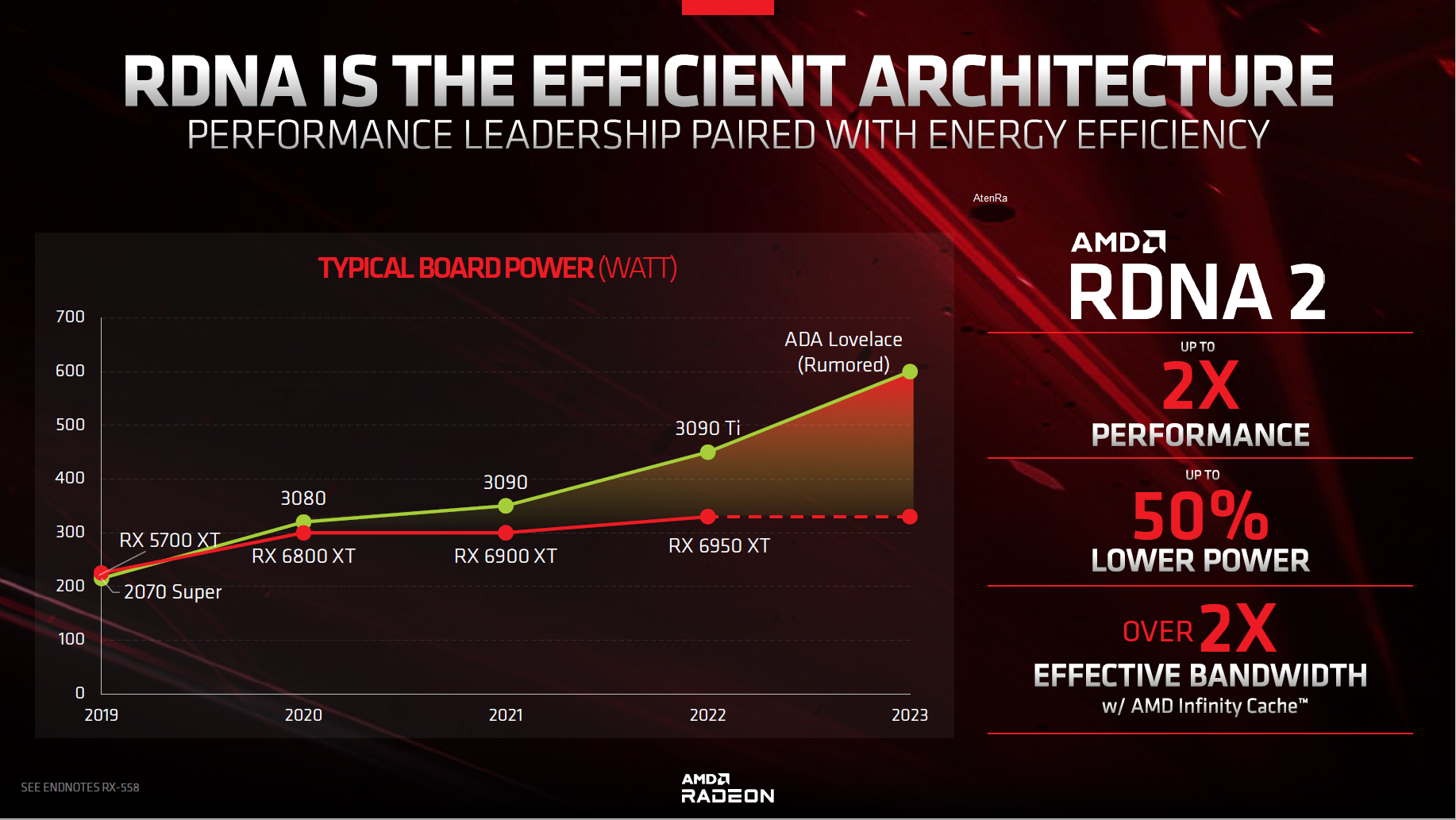
Can we draw a conclusion from the slide bellow that top RDNA3 sku (7950XT ???) will have same TBP of 335W as RX6950XT ???

RDNA-2023.png
 
  • Like
Reactions: Tlh97 and Tarkin77

Aapje

Golden Member
Mar 21, 2022
1,378
1,853
106
In reality, the 6950 uses more power than the 3090, so they are lying. I expect the higher clocks to pull up the power consumption for the next gen, although they should be below Lovelace.

The 6950 is a very inefficiently overclocked card and it's very feasible that the non-overclocked (or less overclocked) 7900 will consume the same. Comparing an overclocked card to a non-overclocked card is a good way to hide a consumption increase through a false comparison.
 
  • Like
Reactions: xpea