- Mar 27, 2009
- 12,968
- 221
- 106
C.B., have you seen the latest on non-volatile MRAM?
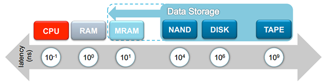
Some info I found on Everspin. Apparently this is a low latency form of non-volatile memory that the company has arranged into the form of a DIMM (Sporting DDR3 speeds on the 90nm process.)
http://www.extremetech.com/computin...ic-ram-thats-500-times-faster-than-nand-flash
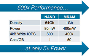
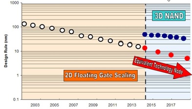
Notice the density difference. I am assuming this is comparing equivalent die sizes on the same process (but this should be verified and checked out).
http://semiaccurate.com/2012/11/16/everspin-makes-st-mram-a-reality/ (Good article. Mentions the 16x density increase possible when switching from 90nm process to 22/20nm process.)
http://www.computerworld.com/s/arti...ST_MRAM_memory_with_500X_performance_of_flash (Mentions Phase change and Memristor as other forms of Non-volatile memory on page 2 of the article.)
Last edited: