[Reuters]Nvidia to use Samsung's 14nm process?

Elixer

Lifer
May 7, 2002
10,371
762
126
Didn't see this posted...
http://www.reuters.com/article/us-samsung-elec-nvidia-idUSKCN10N0L0
Tech giant Samsung Electronics Co Ltd won a contract manufacturing order to make new graphics processing unit (GPU) products for U.S.-based Nvidia Corp, South Korea's Chosun Biz newspaper reported on Friday, citing unnamed sources.

The paper said Samsung would start making the next-generation GPUs using its 14-nanometre production technology before year-end, based on the U.S. company's Pascal architecture. It did not specify the value of the order.

A Samsung Electronics spokeswoman declined to comment, while Nvidia could not be immediately reached for comment.
If this is actually true, it could be for the mobile line...or they are testing the waters to have more fabs available to produce more chips.
 

alcoholbob

Diamond Member
May 24, 2005
6,386
463
126
Sounds interesting. From what I understand with Apple chips TSMC's 16nm versions used less power than Samsung's 14nm chips so it might be due to lower costs.
 

raghu78

Diamond Member
Aug 23, 2012
4,093
1,476
136
So Nvidia is now fabbing GPUs at different foundry processes. This also means they will not be limited by TSMC supply. Nvidia can now roll out the entire Pascal stack before year end with high volume . AMD is going to be slaughtered just like in the Maxwell generation. AMD needs a Polaris revision to fix clock/power issues and a strong Vega lineup. I think AMD might also be fabbing at Samsung in 2017. AMD's wafer purchases at GF in Q2 2016 were extremely low at USD 85 million. So there is a possibility that AMD might be ramping at Samsung as GF messed up pretty bad once again with their 14LPP implementation.

http://www.forbes.com/sites/patrick...14nm-manufacturing-with-samsung/#1ee11b1850fb
 

boozzer

Golden Member
Jan 12, 2012
1,549
18
81
if amd can't ramp up their production, their entire point of going after mid + main stream gpus just went up in smoke.
 

Elixer

Lifer
May 7, 2002
10,371
762
126
if amd can't ramp up their production, their entire point of going after mid + main stream gpus just went up in smoke.
That is the problem with both camps, they aren't getting good enough yields to be able to sell enough chips.

GloFlo should be able to churn out at least 60K wafers per month (http://globalfoundries.com/about/manufacturing/fab-8-overview), but, for whatever reason, even with AMD trying to stockpile before the launch, they still can't produce enough good chips to meet demand. The overall quality of said chips aren't looking too good either going by the ASIC numbers floating around in the forums.

Samsung's fabs can do 2.5million wpm, and of course, lots of that is used for their own products, but they got extra to spare for both nvidia & AMD.

Looks like nvidia is not happy with TSMC's yields either, since they are now looking at samsung for help.
 

Stuka87

Diamond Member
Dec 10, 2010
6,240
2,559
136
Its most likely for mobile chips. As the current desktop chips cannot be simply "moved" to a different process. But if nVidia is indeed powering the Nintendo NX, this could be where those chips will be fabbed.
 

Samwell

Senior member
May 10, 2015
225
47
101
Didn't see this posted...
If this is actually true, it could be for the mobile line...or they are testing the waters to have more fabs available to produce more chips.

Yes it's for Gp107 and GP108 and they are already in production as Huang mentioned in the conference call.
 

Azix

Golden Member
Apr 18, 2014
1,438
67
91
Yes it's for Gp107 and GP108 and they are already in production as Huang mentioned in the conference call.

that could put nvidia months behind on a response to the 470/460. Luckily for them, AMD pricing is funky with many AIB partners. It would also give AMD an opening for affordable gaming laptops with polaris 11.
 

DidelisDiskas

Senior member
Dec 27, 2015
233
21
81
....AMD is going to be slaughtered just like in the Maxwell generation....

Does every thread have to include grandiose terminology about some company being a "joke", or getting killed in some way. This just seems so unnecessary in a tech orientated forum.
 
  • Like
Reactions: Rifter

dark zero

Platinum Member
Jun 2, 2015
2,655
140
106
That is the problem with both camps, they aren't getting good enough yields to be able to sell enough chips.

GloFlo should be able to churn out at least 60K wafers per month (http://globalfoundries.com/about/manufacturing/fab-8-overview), but, for whatever reason, even with AMD trying to stockpile before the launch, they still can't produce enough good chips to meet demand. The overall quality of said chips aren't looking too good either going by the ASIC numbers floating around in the forums.

Samsung's fabs can do 2.5million wpm, and of course, lots of that is used for their own products, but they got extra to spare for both nvidia & AMD.

Looks like nvidia is not happy with TSMC's yields either, since they are now looking at samsung for help.
Samsung will likely help only in the Nintendo NX chip, but that's all.... I see nVIDIA asking Intel for even more help.
 

tviceman

Diamond Member
Mar 25, 2008
6,734
514
126
www.facebook.com
Glofo is a mirror of Samsung, so this lays to rest the theory that Glofo is responsible for P10 and P11 coming up short in every technical metric, unless supply is so constrained at TSMC that they can't take increase capacity to accommodate more orders.
 

raghu78

Diamond Member
Aug 23, 2012
4,093
1,476
136
Glofo is a mirror of Samsung, so this lays to rest the theory that Glofo is responsible for P10 and P11 coming up short in every technical metric, unless supply is so constrained at TSMC that they can't take increase capacity to accommodate more orders.

Glo fo 14LPP is a copy smart of Samsung 14LPP and not a copy exact as Intel does at its fabs. So no you are wrong when you say that its the same.

http://www.extremetech.com/computin...uddy-up-for-14nm-while-ibm-heads-for-the-exit

"Last week, Samsung and GlobalFoundries announced that they would partner together to deploy Samsung’s 14nm technology at all GF facilities. The deal is unprecedented in modern foundry history, with GF essentially acknowledging the two companies will use a “copy-smart” approach that involves synchronizing materials, process recipes, and tools. That’s not quite the level of duplication that Intel’s “copy exactly” approach uses, but it should still allow designs built at one foundry to ramp up smoothly at another."
 

tviceman

Diamond Member
Mar 25, 2008
6,734
514
126
www.facebook.com
Close enough, it sounds like to me. All the evidence I need to see that Glofo is not responsible for Polaris missing performance and perf/w targets. Nvidia shouldn't have any problems keeping Pascal as efficient on Samsung as it is on TSMC.
 

raghu78

Diamond Member
Aug 23, 2012
4,093
1,476
136
Close enough, it sounds like to me. All the evidence I need to see that Glofo is not responsible for Polaris missing performance and perf/w targets. Nvidia shouldn't have any problems keeping Pascal as efficient on Samsung as it is on TSMC.

TSMC has claimed 16FF+ transistor performance is 10% higher than Samsung 14LPP. I think more than that the yields at TSMC are easily the best among foundries especially the parametric yield loss I think is the lowest among foundries.

http://www.inf.usi.ch/faculty/papadopoulou/publications/bookchapter08.pdf

You have to realize that a full process node jump bring 30% performance improvement in transistor performance at same power or 50% power reduction at same transistor performance. So TSMC's performance lead in transistor performance is almost a half node like jump. I am sure Pascal at TSMC 16FF+ will be unbeatable in terms of perf/watt and pascal at Samsung 14LPP will be significantly lower in perf/watt (atleast 20% lower).
 

AtenRa

Lifer
Feb 2, 2009
14,003
3,362
136
Close enough, it sounds like to me. All the evidence I need to see that Glofo is not responsible for Polaris missing performance and perf/w targets. Nvidia shouldn't have any problems keeping Pascal as efficient on Samsung as it is on TSMC.

Just out of curiosity, what perf and perf/w targets are those ??? do you have any link (published before official Polaris release) to point out those targets ??
 

Headfoot

Diamond Member
Feb 28, 2008
4,444
641
126
Close enough, it sounds like to me. All the evidence I need to see that Glofo is not responsible for Polaris missing performance and perf/w targets. Nvidia shouldn't have any problems keeping Pascal as efficient on Samsung as it is on TSMC.

Unless you have a source you don't know that. My guess, which is exactly as good as yours, is that both Glofo and AMD had a role to play in Polaris performance and perf/watt
 

dark zero

Platinum Member
Jun 2, 2015
2,655
140
106
I bet that nVIDIA would be the best absolutely if they were made in Intel process.

NVIDIA should ally with Intel if they want to be invincible.
 

tviceman

Diamond Member
Mar 25, 2008
6,734
514
126
www.facebook.com
Just out of curiosity, what perf and perf/w targets are those ??? do you have any link (published before official Polaris release) to point out those targets ??

Common sense, that is all we need. The last time AMD released a ~220-230mm2 chip on the previous manufacturing process, it consumed 40% less power (see here: https://www.techpowerup.com/reviews/AMD/HD_7850_HD_7870/24.html ) and had 10-12% more OC headroom (see here: https://www.techpowerup.com/reviews/AMD/HD_7850_HD_7870/29.html ) than Polaris 10. Compared to the competition then and now, it was 10% faster at release AND more efficient than Nvidia's comparable offering vs. today generally losing and consuming 25% more power. Compared to Nvidia's next bigger chip, THEN Nvidia was only 30% faster whereas now Nvidia is 80% faster. AMD didn't just lose ground, they failed to show up to the race.

Slice it however you want. If P10 and P11 met their internal technical goals, the bar was VERY, VERY low. Glofo didn't screw the pooch on this one, not when they're mirroring what Samsung is doing and Nvidia is happily moving some if it's products over to Samsung.
 

Stuka87

Diamond Member
Dec 10, 2010
6,240
2,559
136
Samsung will likely help only in the Nintendo NX chip, but that's all.... I see nVIDIA asking Intel for even more help.

Being that Intel and nVidia do not get along, I do not see Intel helping them in any way.
 

Magee_MC

Senior member
Jan 18, 2010
217
13
81
Being that Intel and nVidia do not get along, I do not see Intel helping them in any way.
I thought that they got along well enough for Intel to license their GPU patents. As I understand it, they're negotiating an extension of that license, so they have a working relationship on some level.

Maybe Intel could use access to their fabs to smooth the license negotiations. I don't know that this is what's happening, but just throwing it out there as one possibility that could induce both companies to work together on specific technologies outside of their areas of competition.
 

AtenRa

Lifer
Feb 2, 2009
14,003
3,362
136
Common sense, that is all we need. The last time AMD released a ~220-230mm2 chip on the previous manufacturing process, it consumed 40% less power (see here: https://www.techpowerup.com/reviews/AMD/HD_7850_HD_7870/24.html ) and had 10-12% more OC headroom (see here: https://www.techpowerup.com/reviews/AMD/HD_7850_HD_7870/29.html ) than Polaris 10. Compared to the competition then and now, it was 10% faster at release AND more efficient than Nvidia's comparable offering vs. today generally losing and consuming 25% more power. Compared to Nvidia's next bigger chip, THEN Nvidia was only 30% faster whereas now Nvidia is 80% faster. AMD didn't just lose ground, they failed to show up to the race.

Slice it however you want. If P10 and P11 met their internal technical goals, the bar was VERY, VERY low. Glofo didn't screw the pooch on this one, not when they're mirroring what Samsung is doing and Nvidia is happily moving some if it's products over to Samsung.


HD6970 @ 40nm
Die size 389mm2, 2640M Transistors , 250W TDP

HD7870 @28nm
Die size 212mm2, 2800M Transistors , 175W TDP

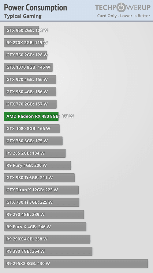
Power Consumption
power_average.gif


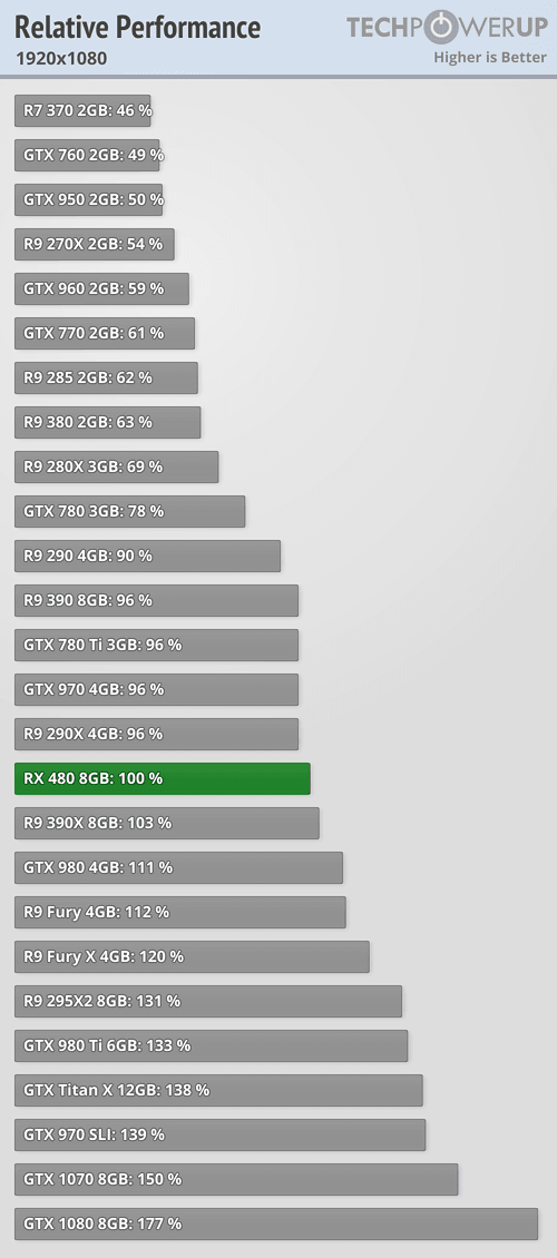
perfrel_1920.gif


HD7870 vs HD6970

Transistors = 6% more
Die size = 45,5% smaller
TDP = 30% less
Power Consumption = 103W-184W = 44% less
Performance = 10% faster


------------------------


R9 390X @ 28nm
Die size 438mm2, 6200M Transistors , 275W TDP

RX 480 @28nm
Die size 232mm2, 5700M Transistors , 150W TDP

Power Consumption
power_average.png


perfrel_1920_1080.png


RX 480 vs R9 390X

Transistors = 8% less
Die size = 47% smaller
TDP = 45,5% less
Power Consumption = 163W-264W = 38% less
Performance = 3% slower

Pretty much the same as going from 40nm to 28nm, they managed to have almost the same perf with 8% less transistors at 45% lower TDP and 38% lower power consumption when HD7870 had 6% more transistors than HD6970. It is clear the targets for Polaris 10 were , smaller die as possible with lower TDP as possible at the same performance as R9 390X.
Also, TPU use way too much GameWorks games and they measure power consumption in an old 2012 DX-11 game. perf/watt in DX-12 games between RX 480 vs R9 390X will be even higher.

But that doesn't change the fact that you had no idea what the official targets were for Polaris 10 and "common sense" is not an evidence of "missing" official performance and perf/watt targets.

Edit: And one last and extremely important aspect, we dont know what the R&D target was for Polaris.
 
Last edited:

tviceman

Diamond Member
Mar 25, 2008
6,734
514
126
www.facebook.com
RX 480 vs R9 390X

Transistors = 8% less
Die size = 47% smaller
TDP = 45,5% less
Power Consumption = 163W-264W = 38% less
Performance = 3% slower

Pretty much the same as going from 40nm to 28nm, they managed to have almost the same perf with 8% less transistors at 45% lower TDP and 38% lower power consumption when HD7870 had 6% more transistors than HD6970. It is clear the targets for Polaris 10 were , smaller die as possible with lower TDP as possible at the same performance as R9 390X.
Also, TPU use way too much GameWorks games and they measure power consumption in an old 2012 DX-11 game. perf/watt in DX-12 games between RX 480 vs R9 390X will be even higher.

But that doesn't change the fact that you had no idea what the official targets were for Polaris 10 and "common sense" is not an evidence of "missing" official performance and perf/watt targets.

Edit: And one last and extremely important aspect, we dont know what the R&D target was for Polaris.

A market replacement is not the same as a successor. Pitcairn wasn't the successor to Cayman, and Polaris isn't the successor to Hawaii. You're comparing a 512-bit 440mm2 former flagship chip to a 256-bit 230mm2 mid-range chip. PLEAAAASE. RX 480 didn't even match Hawaii in performance. You know that plain and simple. You're picking a resolution that highly favors Polaris and gimping Hawaii. It just shows you're skewing information in an attempt to back up your narrative. We both can play the game of making certain comparisons which highly favor a particular narrative, or we can just use common sense and compare chips from different family's from their hierarchical perspective. Whatever floats your boat and helps you sleep better at night!

In the meantime, we'll just wait on the new chips from Nvidia to come out, paint us a perf/w picture, and play the Polaris blame game some more with a new set of rules that AMD die hard fans will come up with.
 
  • Like
Reactions: Phynaz and Sweepr