Discussion RDNA 5 / UDNA (CDNA Next) speculation

Page 40 - Seeking answers? Join the AnandTech community: where nearly half-a-million members share solutions and discuss the latest tech.

ToTTenTranz

Senior member
Feb 4, 2021
547
972
136
Note Omdia describe the Steam Deck as being the PC handheld market leader yet completely eclipsed by Nintendo.

The sum total of all PC handheld sales yearly is a mere fraction of Switch 1/2.

Comparison to Switch is irrelevant. Steam's main platform isn't handhelds. The Deck is simply yet another form factor for which they can take a 30% cut out of every software sale.
It's growth for their 20 year-old store, not a main bread winner for which their existence depends on. Unlike Nintendo.

In the off chance you guys believe Valve are kicking themselves in the back for not competing with Nintendo in Deck volume sales: they're not.
 
  • Like
Reactions: marees

gdansk

Diamond Member
Feb 8, 2011
4,432
7,465
136
In the off chance you guys believe Valve are kicking themselves in the back for not competing with Nintendo in Deck volume sales: they're not.
I'm just telling you AMD needn't care.
If that source is realistic the TAM for PC handhelds chips is tiny (maybe $600-700 million a year by 2029).
That is hand me down or pay for custom chip territory.
 

Joe NYC

Diamond Member
Jun 26, 2021
3,455
5,047
136
There's
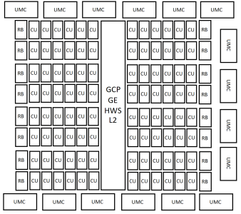
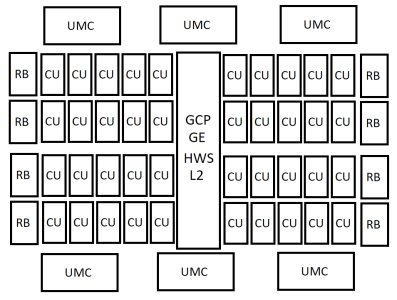
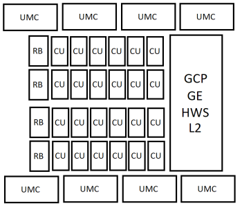
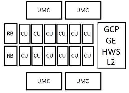
- Medusa Halo with SoC (CPU + I/O) and AT3 GMD (GPU + Memory)
- Medusa Premium with smaller SoC (CPU + I/O) and AT4 GMD (GPU + Memory)
- Medusa Point with SoC (CPU + GPU + Memory + I/O) plus optional CCD.

Lots of SoCs. Interesting that Medusa Halo and Medusa Premium have separate dies - for not exactly high volume products. Probably only makes sense (from volume perspective) if these are shared with consoles.

Medusa Halo should also have optional CCD, which would mean 3 chip CPU.

MLID said all of the CCDs are V-Cache compatible. Which would leave Medusa Premium one SKU without V-Cache capability.
 

Joe NYC

Diamond Member
Jun 26, 2021
3,455
5,047
136
Well, no, because nothing AMD ships is a 10W tablet part.

If current Steam Deck is 8x RDNA 2 CUs, 8x RDNA 5 CUs would be some upgrade, even with just the main laptop SoC. Better efficiency from RDNA5, better power efficiency with new process node nodes and higher clocks, LPDDR6.

Maybe not enough of an upgrade but some. Maybe ~1.75x performance increase.

And Valve could make their own "console" with Medusa Premium.
 

adroc_thurston

Diamond Member
Jul 2, 2023
6,386
8,999
106
If current Steam Deck is 8x RDNA 2 CUs, 8x RDNA 5 CUs would be some upgrade, even with just the main laptop SoC. Better efficiency from RDNA5, better power efficiency with new process node nodes and higher clocks, LPDDR6.
can you like read?
AMD is not shipping 10W tablet parts anymore.
They're gone-gone.

That's why Valve begged AMD for a semicustom slot.
 

ToTTenTranz

Senior member
Feb 4, 2021
547
972
136
I'm just telling you AMD needn't care.
They don't need to. They just need to sell Medusa Premium SoCs to OEMs.


Well, no, because nothing AMD ships is a 10W tablet part.
That only means the Steam Deck 2 will be using a 15-25W solution, not that the Deck 2 can't exist.
Which isn't bad per se. People with a $400 budget can just go get a Switch 2 nowadays, and most of Valve's Deck sales come from the >$600 models anyway.
 

Mopetar

Diamond Member
Jan 31, 2011
8,463
7,683
136
Preeetty sure that battery life still has something to say about that.

You might be able to get around the thermal issue, but the reduced battery volume in an ultra thin is still a thing.

Is it an actual issue for most users and their workloads though? There's a difference between having a platform capable of operating at 25W and it actually sustaining that under regular use cases.

Most of the time it will be drawing much less power because a word processor isn't all that resource intensive. Neither is web browsing when scripts are disabled and ads/trackers are blocked.

Companies could use a 10W part, but it'll get smoked in benchmarks and everyone will buy the 25W competitor product. The extra oomph is great when needed, even if it's not needed all that often. The battery life difference only shows up if both systems are pegged at 100%, but that can be misleading itself if the 10W part gets less overall work done. For x86 CPUs, 25W is already so far down the performance/watt curve that efficiency gains for reducing power further are negligible and may even be worse since there's always some baseline minimum of power just to have the system on and getting work done faster and returning to idle is overall more efficient.
 

Magras00

Member
Aug 9, 2025
40
91
46
Man RDNA5 just keeps getting wilder and wilder. I'm just baffled by the incredibly low L2 capacities.

AT2 with 36gbps G7 still falls short of 5070 TI's mem BW and halves L2 (24MB vs 48MB).
Despite that it could easily bury 4090 (+37-40% 9070XT raster) if AMD pushes clocks.

Full AT2 matching GB202 spec with half the L2 is impressive especially with AT2 extrapolated perf at ~50-60% ahead of 5090.

And the low L2 for LPDDR based cards is even more impressive but then again 384bit LPDDR6 12000 = 570ish GB/S halfway between 4070 TI and 9070XT. LPDDR6 has mandatory ECC that reduces BW by 11.1% so this isn't accurate. It's closer to 4070 TI and nowhere near 9070XT.

Is this low L2 a result of the new decentralized SE level scheduling paradigm @Kepler_L2?
That is the only explanation I can think of that could have such a drastic impact. ADC and WGS within SEs + Local launchers mean that all caches effectively move up one tier. L0 now acts as both L1 and L0 (WGP self launch), L1 acts as L2 (ADC + WGS) and L2 is now nothing more than a work item victim cache.
Performing all scheduling and dispatch at the Shader Engine level instead of orchestrated through a central command processor means that with the exception of occasional scratch buffer L2 spillovers only work item data resides in L2.

Please correct me if this observation is incorrect.

SKU spec table​

SKUCUs (new/old)L2 (MB)PHY typeMem bus (bit)SE/SACU/SE (new/ old)
AT096/19264GDDR75128/1612/24
AT240/8024GDDR71924/810/20
AT324/4832LPDDR5X/6256/3842/412/24
AT412/2416LPDDR5X/?6128/?1921/212/24
 
Last edited:

Kepler_L2

Senior member
Sep 6, 2020
967
4,011
136
Man RDNA5 just keeps getting wilder and wilder. I'm just baffled by the incredibly low L2 capacities.

AT2 with 36gbps 7 still falls short of 5070 TI's mem BW and halves L2 (24MB vs 48MB).
Despite that it could easily bury 4090 (+37-40% 9070XT raster) if AMD pushes clocks.

Full AT2 matching GB202 spec with half the L2 is impressive especially with AT2 extrapolated perf at ~50-60% ahead of 5090.

And the low L2 for LPDDR based cards is even more impressive but then again 384bit LPDDR6 12000 = 570ish GB/S halfway between 4070 TI and 9070XT.

Is this low L2 a result of the new decentralized SE level scheduling paradigm @Kepler_L2?
That is the only explanation I can think of that could have such a drastic impact. ADC and WGS within SEs + Local launchers mean that all caches effectively move up one tier. L0 now acts as both L1 and L0 (WGP self launch), L1 acts as L2 (ADC + WGS) and L2 is now nothing more than a work item victim cache.
Performing all scheduling and dispatch at the Shader Engine level instead of orchestrated through a central command processor means that with the exception of occasional scratch buffer L2 spillovers only work item data resides in L2.

Please correct me if this observation is incorrect.

SKU spec table​

SKUCUs (new/old)L2 (MB)PHY typeMem bus (bit)SE/SACU/SE (new/ old)
AT096/19264GDDR75128/1612/24
AT240/8024GDDR71924/810/20
AT324/4832LPDDR5X/6256/3842/412/24
AT412/2416LPDDR5X/?6128/?1921/212/24
If MI400 is any indication they have massively increased CU local caches
 

Saylick

Diamond Member
Sep 10, 2012
3,975
9,309
136
If MI400 is any indication they have massively increased CU local caches
How much local cache does it have again? And it's dynamically allocated, right? If so, it appears AMD's cache system is heading towards what Nvidia has had for a while now.

I am a little busy at the moment, but would be nice if someone could do a comparison of the total amount of L0, L1, L2, and MALL between RDNA 3, 4, and what we think will be for RDNA 5.
 
  • Like
Reactions: Tlh97 and Magras00

Magras00

Member
Aug 9, 2025
40
91
46
How much local cache does it have again? And it's dynamically allocated, right? If so, it appears AMD's cache system is heading towards what Nvidia has had for a while now.

I am a little busy at the moment, but would be nice if someone could do a comparison of the total amount of L0, L1, L2, and MALL between RDNA 3, 4, and what we think will be for RDNA 5.

CDNA 3 = 64KB LDS and CDNA 4 = 160KB LDS/2.5X.
NVIDIA Blackwell DC is still at 256KB L1 or 228KB shared cache.

CU/SM level caches is def where AMD has a major deficit on consumer as well:
RDNA 4 LDS (WGP) = 128KB, 64KB per CU + extra caches while NVIDIA Ampere and later = 128KB/SM

For consumer 2.5X = 320KB per GFX13 CU. They also need to up L1 to avoid spillover from local scratch buffer to L2. Prob how GFX13 manage most of the L2 shrink, but likely some clever compression and data management wizardry as well.

Maybe GFX13 unifies everything on the CU level into one big L1/LDS and L0 like NVIDIA has had since Turing. Maybe even unified Register file.
Whatever ends up happening if they're serious about localized scheduling and shrink L2 by that much (9070XT 64MB -> AT2 24MB) prob there's no way around beefed up LDS and L1, question is how large will they be.

AMD cache hierarchy and GFX13 speculation

Like Kepler has said before MALL is deprecated with RDNA 5. Also AMD's L1 is called LDS or shared memory, the L1 is mid tier cache between LDS and L2, if NVIDIA had one one it would probably be called L1.5. Would like to see that as well.
My baseless speculation for RDNA 5 CU is 92KB L0, 256-384KB LDS + 384-512KB L1 per shader array.
 
Last edited:
  • Like
Reactions: Tlh97

Kepler_L2

Senior member
Sep 6, 2020
967
4,011
136
How much local cache does it have again? And it's dynamically allocated, right? If so, it appears AMD's cache system is heading towards what Nvidia has had for a while now.

I am a little busy at the moment, but would be nice if someone could do a comparison of the total amount of L0, L1, L2, and MALL between RDNA 3, 4, and what we think will be for RDNA 5.
CDNA4 is 32KB L0 + 160KB LDS, CDNA5 is 448KB Shared L0/LDS
 

Magras00

Member
Aug 9, 2025
40
91
46
CDNA4 is 32KB L0 + 160KB LDS, CDNA5 is 448KB Shared L0/LDS

Is RDNA5 taking this even further like Apple's M3? https://developer.apple.com/videos/play/tech-talks/111375/ (from 11:37)

Looks like M3 and A17 Pro has flexible on-chip memory that basically treats all shader core local memory as one big pool of cache that can be dynamically assigned to maximize performance for each workload.

"And now that register, threadgroup, tile, stack, and buffer data are all cached on chip. This has allowed us to redesign the on-chip memories into fewer larger caches that service all these memory types. This flexibility will benefit shaders that don't make heavy use of each memory type. In the past, if a compute kernel didn't use, for example threadgroup memory, its corresponding on-chip storage would go completely unused. Now the on-chip storage will be dynamically assigned to the memory types that are used by your shaders giving them more on-chip storage than they had in the past, and ultimately better performance"

And now for specific workloads:

"For example, for shaders with heavy register usage, that may mean higher occupancy. For shaders that repeatedly access a large working set of buffer data, that will mean better cache hit rates, lower buffer access latency and thus better performance. And for apps that make heavy use non-inline functions, such as function pointers, visible function tables, and dynamically linekd shader libraries this means more on-chip stack space to pass function parameters and thus faster function calls."

M3 and A17 Pro even has thread occupancy management to avoid cache spillovers to higher level caches. Maybe this is also part of how RDNA5 shrinks L2.
 
Last edited:

Saylick

Diamond Member
Sep 10, 2012
3,975
9,309
136
Oh noes, they're heading to where Apple is.
CDNA4 is 32KB L0 + 160KB LDS, CDNA5 is 448KB Shared L0/LDS
So less levels of cache, but each level is bigger and dynamically allocated (ideally completely handled by the hardware and without developer input)? If so, this is a very smart way of utilizing a limited amount of cache efficiently.
 
  • Like
Reactions: Tlh97 and Magras00

Timorous

Golden Member
Oct 27, 2008
1,975
3,858
136
Cache costs cash, got it.

That is the exact reason I didn't believe the cache rumours for RDNA2. It seemed like going with a wider bus would cost less die area to achieve similar performance goals so if AMD were willing to spend 500mm of die area then going with a wider bus and adding more shader cores would be better balanced overall than a huge chunk of MALL.