
Glo.
Diamond Member
- Apr 25, 2015
- 5,930
- 4,991
- 136
Guys, I know this is a bit stretched out comparison, however. The Vega GPU averaged well over 60 FPS in 4K doom right? We can say that it more likely averaged around 70 FPS in this resolution.
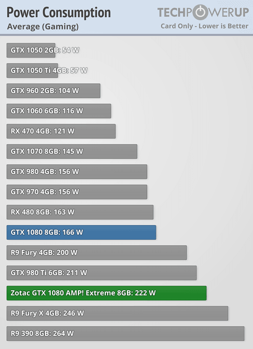
I wanted to check how it compares to GTX 1080 Zotac AMP! Extreme version. The GPU that draws 222W on average in games:
What was the score?
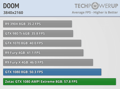
58 FPS on average in Doom 4K Vulkan, on a platform with 6700K OC'ed to 4.5 GHz.
AMD demo platform was using Ryzen(?) CPU.
I wanted to check how it compares to GTX 1080 Zotac AMP! Extreme version. The GPU that draws 222W on average in games:
What was the score?
58 FPS on average in Doom 4K Vulkan, on a platform with 6700K OC'ed to 4.5 GHz.
AMD demo platform was using Ryzen(?) CPU.
