Performance per Watt: What chance does Polaris have?

Page 4 - Seeking answers? Join the AnandTech community: where nearly half-a-million members share solutions and discuss the latest tech.

Good_fella

Member
Feb 12, 2015
113
0
0
IIRC, Intel is already shipping to select customers building super computers.

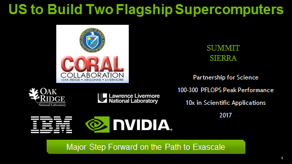
Look at that pic though, contracts for 100 >PFlops. Probably rising fast too.

That's what NV is afraid of. Not AMD. :)

coral_summit_sierra_supercomputers.png


So it is not required. A gimmick then?


Threadcrapping and trolling are not allowed
Markfw900

If NVlink is gimmick then AMD's Coherent Interconnect Fabric is gimmick too.
 

RussianSensation

Elite Member
Sep 5, 2003
19,458
765
126
AMD should just shrink Hawaii and add it some optimizations.

They are going to do much better than that because Polaris 10 is a heavily redesigned GCN 4.0 architecture. That means it won't just be a shrunken Hawaii with perf/watt optimizations. For HPC market, with 16GB HBM2, Vega should be ready to go. Fury X already has 8.6Tflops of FP32. If Vega retains 4096 SPs of Fury X and 14nm node allows AMD to raise GPU clocks from 1050 to 1300mhz, that matches P100's FP32 performance already. AMD's issue in HPC space is not raw performance but software/platform developer support. NV basically started HPC market with G80 so it'll take a lot of time for this market to convert to OpenCL. On the positive side, AMD's GCN were already compute powerhouses so AMD doesn't need to waste much time and transistor space on focusing on compute this generation. That's why they have a real shot of actually surpassing nV if they decide to make a 550-600mm2 VEGA HBM2 with gaming focus and some ludicrous 5120-6144 shaders.

That's why so many people in the P100 thread are now hypothesizing GP104/102 to have 4096-6144 CUDA cores since one can sense they fear AMD going all in on gaming performance considering GCN has Async Compute in the bank from the start. I think it's fair to say almost no one expected 610mm2 16nm Pascal to have only 3840 CUDA core and 240 TMUs....
 

xpea

Senior member
Feb 14, 2014
429
135
116
They are going to do much better than that because Polaris 10 is a heavily redesigned GCN 4.0 architecture. That means it won't just be a shrunken Hawaii with perf/watt optimizations. For HPC market, with 16GB HBM2, Vega should be ready to go. Fury X already has 8.6Tflops of FP32. If Vega retains 4096 SPs of Fury X and 14nm node allows AMD to raise GPU clocks from 1050 to 1300mhz, that matches P100's FP32 performance already. AMD's issue in HPC space is not raw performance but software/platform developer support. NV basically started HPC market with G80 so it'll take a lot of time for this market to convert to OpenCL. On the positive side, AMD's GCN were already compute powerhouses so AMD doesn't need to waste much time and transistor space on focusing on compute this generation. That's why they have a real shot of actually surpassing nV if they decide to make a 550-600mm2 VEGA HBM2 with gaming focus and some ludicrous 5120-6144 shaders.

That's why so many people in the P100 thread are now hypothesizing GP104/102 to have 4096-6144 CUDA cores since one can sense they fear AMD going all in on gaming performance considering GCN has Async Compute in the bank from the start. I think it's fair to say almost no one expected 610mm2 16nm Pascal to have only 3840 CUDA core and 240 TMUs....
number of ALUs and theoretical peak FLOPS are not the only relevant metric. moar ALUs are great for marketers and noobs, but solid register topology (large file and fast access) + LDS atomics are more important for real sustain compute performance. Exact GP100 focus...
so don't be so sure that Vega will "easily" beat Pascal in compute with only moar ALUs. Until independent test, better be prudent.
 

Adored

Senior member
Mar 24, 2016
256
1
16
Hawaii doesn't have delta color compression so the shrink would be mostly wasted, or at least the huge 512-bit bus would be a waste. I doubt we'll ever see that again.
 

RussianSensation

Elite Member
Sep 5, 2003
19,458
765
126
number of ALUs and theoretical peak FLOPS are not the only relevant metric. moar ALUs are great for marketers and noobs, but solid register topology (large file and fast access) + LDS atomics are more important for real sustain compute performance. Exact GP100 focus...
so don't be so sure that Vega will "easily" beat Pascal in compute with only moar ALUs. Until independent test, better be prudent.

I presume this time AMD will make a better balanced chip with 96/128 ROPs and a heavily upgraded geometry engine/front end. I am not saying that Vega will beat Pascal but this is the best chance AMD has because it looks like Pascal took a massive transistor/die size hit by tacking on compute functionality that GCN mostly had already. The 2 question marks are if AMD's flagship will actually have > 4096 SPs and will AMD's large die chips hit 1450-1500mhz stock Boost clocks like GP100 has? You are right that having more ALUs doesn't mean success if the competitor's cards have 25-30% overclocking headroom.

Out of the box though, Fury X beats Titan X at 4K. If Vega is wide (>4096 SPs) and can overclock well, the major advantage (OCing) that 980Ti/TX held over Fury X will be evaporated. That's my point but whether AMD can deliver is another story as you know. :D

perfrel_3840_2160.png
 

Mahigan

Senior member
Aug 22, 2015
573
0
0
number of ALUs and theoretical peak FLOPS are not the only relevant metric. moar ALUs are great for marketers and noobs, but solid register topology (large file and fast access) + LDS atomics are more important for real sustain compute performance. Exact GP100 focus...
so don't be so sure that Vega will "easily" beat Pascal in compute with only moar ALUs. Until independent test, better be prudent.

I think you're just throwing around words here. Register topology?? Are you simply mentioning this buzzword because of the P100 unveiling? P100 has 256KB registers per SM. Same as Maxwell/Kepler. What P100 did differently was reduce the amount of FP32 CUDA cores per SM but add many more SMs. That's why P100 has 14MB worth of register spacing. 256KBx56.

What does GCN have? 256KB Register spacing per CU. How many CUs in Fiji? 64. 64 x 256KB? 16MB. How many SIMD cores per CU? 64 (4x16).

What's important for sustained compute performance? Depends on what you mean. Do you mean concurrent Warps? Then what's important is the register spacing, but that's remained the same per SM from Kepler all the way to Pascal, so 64 concurrent Warps Maximum. But what's important in keeping sustained performance up to 64 concurrent Warps? Local Caches. This is where P100 improves. There's 64KB worth of Shared Local Data Cache within each SM as well as the L1/Texture cache. That's the same as Maxwell but since there is less logic per SM then there's more cache available to each individual SIMD/Texture Unit etc. This prevents a cache spill into L2 cache.

But guess what? GCNs CUs have more cache even still and can sustain 40 concurrent wavefronts. Maxwell dropped off after 16 Warps.

Plz don't tell me we'll be hearing "register size" as a new talking point... :/
 

Mahigan

Senior member
Aug 22, 2015
573
0
0
Oh and BTW, concurrent Warps/Wavefronts denotes parallelism. This means that Pascal is headed towards a more parallel architecture like...GCN.

If Vega retains its 64 CUs from Fiji with 64 (4x16) SIMD cores each but with improves efficiency then you're looking at 16MB of register space. In total you're looking at 40 Wavefronts (64 threads each or 2,560 threads total) per CU. That's still much higher parallelism than Pascal's 64 Warps (32 threads each or 2,048 threads total). If RTG adds more cache to Vega, per CU, then they easily have Pascal beat in that department. NVIDIA are playing catch up here.

What helped NVIDIA, in gaming scenarios, was the lack of parallelism and the higher Graphics to Compute work ratio. Not Maxwell or Kepler's compute performance which wasn't on par with GCN parallelism wise.

It really looks to me like Vega will beat GP100 because the tweaks needed to GCN are minimal in order to achieve the task. A few efficiency boosts, Large L2 Cache, 128 ROps and more cache per CU and you're there.

Since Pascal will likely lead to more parallel workloads then all GCN cards will gain a boost from Pascal optimized workloads. Face it, NVIDIA have just designed a GCN-like architecture with Pascal.
 

fellix

Junior Member
Jan 30, 2012
4
0
66
4. A scientific paper confirmed my suspicions about Maxwell's lack of parallelism. Theoretically speaking, each Maxwell SM is capable of 64 concurrent Warps and each Warp being made up of 32 threads for a total of 2,048 threads per SM. Sadly, this is not the case in practice. In practice Maxwell loses performance once we move higher than 16 concurrent Warps per SM. This pits the maximum threads per SM, before a performance drop off, at 512 threads.
20172b26638fe3f922eac78b3b1360f2.jpg
Maxwell is thus not a good candidate for Asynchronous compute + graphics even if its static scheduler could emulate the process. On top of that, Maxwell's static scheduler hits the CPU hard when attempting to emulate.
You should probably link to the source of that paper (where the chart is from) and clarify that it has nothing to do with async compute in D3D12. It actually studies a method of microbenchmarking the memory pipeline of modern GPUs and is very informative by the way, spanning three distinct architectures.

About the parallelism in the SM. The number of warps per multiprocessor indicates the ability of the SM scheduler(s) to pick warps immediately from the pool (of 64) and send them for processing, in case of pipeline stall from a previous warp execution (like texture or memory load wait-time). This is done to keep the ALU array bussy with work, not to indicate the ability to execute all the warps at the same time. After all, the SM contains only so much ALUs and GPR space.
 
Last edited:
Feb 19, 2009
10,457
10
76
GCN has been gaining in recent games, DX11 included, so it's power efficiency isn't far behind. If we include a few of the DX12 titles on board, I mean in QB, a 390 is 50-90% faster in gameplay...

Then you have to question WHICH 28nm GCN are you comparing?

Nano is pretty damn efficient.

Some Fury models are also efficient and that's in DX11 games.
 
Feb 19, 2009
10,457
10
76
The one thing we know of, Polaris 11 in Battlefront 60 fps on medium settings drew ~35W, since total system power (with an i7 4770K!) was ~80W.

Obviously it's not running max performance. The rumor SKUs are ~50W, so if it's max, it could hit 380 performance at 50W.

Anybody want to do the maths on perf/w??

380 is what, 150W gaming load? That right there is 3x already.
 

Abwx

Lifer
Apr 2, 2011
10,854
3,298
136
The one thing we know of, Polaris 11 in Battlefront 60 fps on medium settings drew ~35W, since total system power (with an i7 4770K!) was ~80W.

Obviously it's not running max performance. The rumor SKUs are ~50W, so if it's max, it could hit 380 performance at 50W.

Anybody want to do the maths on perf/w??

The 2.5x perf/Watt announced by AMD means nothing in isolation, what is missing is the level at wich this improvement occur as they could had a better ratio unless they dumped some of the potential in increasing the perfs, wich is apparently what they did if we are to compare with GF s published perf/watt numbers.

For instance if they keep the perfs at the same level that the previous gen they will have 3.5x the perf/watt, but if they increase frequencies by 1.4x to grab some perfs the improvement will be reduced by the same 1.4x ratio, that is the announced 2.5x.

As for the TDPs that s straightforward because the "norm" is to not exceed 0.6W/mm2, so this put a 232mm2 chip at 140W max TDP, wich correlate with the numbers i posted elsewhere about the options they have :

- Same perfs and 70W TDP (3.5x the perf/watt).

- 20% better perfs and 105W TDP (2.85x the perf/watt)

- 40% better perfs and 135W TDP (2.5x the perf/Watt)
 

Glo.

Diamond Member
Apr 25, 2015
5,662
4,421
136
Look at teraflops measure. They always take it as a metric for measuring performance per watt.

If we look at 2.5 times Perf/watt from Hawaii that means 2560 GCN core GPU with 1150 MHz core clock rated at 100W or 3072 GCN core chip rated at 1150 MHz at 125W TDP.
 
Last edited:

Abwx

Lifer
Apr 2, 2011
10,854
3,298
136
Look at teraflops measure. They always take it as a metric for measuring performance per watt.

If we look at 2.5 times Perf/watt from Hawaii that means 2560 GCN core GPU with 1150 MHz core clock rated at 100W or 3072 GCN core chip rated at 1150 MHz at 125W TDP.

That s not as simple as perf/watt is a sliding rule depending if you keep the same frequency (so the same perf) or not, because increasing frequency by a ratio X decrease perf/watt by this ratio X..

If we take 1GHz/2560SPs/250W as the starting point then a 2.5x perf/watt improvement could mean 1GHz/2560SPs/100W, that is at the same throughput.

But what if the 2.5x is for 1.4GHz/2560SPs/140W..?.

In this latter case that s 2.5x at 1.4x the throughput, and while it s the same efficency on a consumer POV this has a different meaning for enginers as they know that should the chip being clocked at same throughput then the perf/watt would increase by 1.4x up to 3.5x, wich is the perf/watt improvement of the 14nm LPP at equal frequency in respect of (GF s) 28nm.

Edit : numbers are here, the first slide is a summary of the second one, the 28nm SLP is the process that suit GPUs and wich is used to fab AMD s Kabini/Beema :

UslEg0v.png


I9s2ur3.jpg
 
Last edited:

airfathaaaaa

Senior member
Feb 12, 2016
692
12
81
how can we speculate about the tflop perf since we dont have any clear picture of the new uarch to see how its working? neither of those claims are taking into the account the power gating (the only thing we know)
 

Abwx

Lifer
Apr 2, 2011
10,854
3,298
136
how can we speculate about the tflop perf since we dont have any clear picture of the new uarch to see how its working? neither of those claims are taking into the account the power gating (the only thing we know)

Assuming a GCN 1.4 CU throughput/Hz can be increased by 10% then it will probably require at least 10% more power, so in appearance the perf/watt/Hz will not improve if frequency is left unchanged.

The advantage is that to get the same throughput the GCN 1.3 CU frequency must be raised by 10%, wich will increase its power drain by 21%, hence at equal throughput the new uarch would be 10% more efficient because it use a lower frequency, and that power scale as a... power of 2 in respect of frequency.
 

el etro

Golden Member
Jul 21, 2013
1,581
14
81
I think that Polaris regain the perf/mm2 lead versus Nvidia, even with normalized die sizes.
And perf/w goes to Polaris too, due to 14LPP power advantage over 16FF+(remains to be seen, but i bet that it is).
 

raghu78

Diamond Member
Aug 23, 2012
4,093
1,475
136
I think that Polaris regain the perf/mm2 lead versus Nvidia, even with normalized die sizes. And perf/w goes to Polaris too, due to 14LPP power advantage over 16FF+(remains to be seen, but i bet that it is).

I think Polaris is a huge improvement and I am chosing to believe that Polaris 10 2.5x perf/watt gains are in comparison with Fury X. Others might differ in their opinion and thats fine. I am speculating Fury X perf at 110w with a 2304 sp GDDR5 product and a 15-20% faster flagship Polaris 10 with 2560 sp and GDDR5X. I might be wrong but thats fine. Its just speculation and I am having a go at it. :)
 

el etro

Golden Member
Jul 21, 2013
1,581
14
81
I think Polaris is a huge improvement and I am chosing to believe that Polaris 10 2.5x perf/watt gains are in comparison with Fury X. Others might differ in their opinion and thats fine. I am speculating Fury X perf at 110w with a 2304 sp GDDR5 product and a 15-20% faster flagship Polaris 10 with 2560 sp and GDDR5X. I might be wrong but thats fine. Its just speculation and I am having a go at it. :)

Is what i speculate too, but without GDDR5x. :)
 

Glo.

Diamond Member
Apr 25, 2015
5,662
4,421
136
If you think that Fury X is the goal here, for 2.5 times better power efficiency then you are looking at a GPU with around 75 GFLOPs of compute power per Watt. 3072 GCN4 GPU with 1150 MHz core clock rated at 100W of TDP.

A bit unrealistic IMO.

What that gives me a thought is that AMD's claim of 2.5 times better efficiency was extremely enigmatic. It could meant everything. We do not know the full performance of the GPUs, we do know a bit the power consumption in certain scenarios of those GPUs, but nothing apart from that.

It would be f*****g shocking if AMD would be able to bring 3072 GCN core GPU into 100W range.
 

Abwx

Lifer
Apr 2, 2011
10,854
3,298
136
I think that Polaris regain the perf/mm2 lead versus Nvidia, even with normalized die sizes.
And perf/w goes to Polaris too, due to 14LPP power advantage over 16FF+(remains to be seen, but i bet that it is).

I think so as well, and for several reasons.

One is that GF s announced perf/watt improvements can be summarized (in respect of their own 28nm SLP) as either :

- 0.286x the power at same frequency.

- or 1.989x the frequency at same power.

Second is that TSMC announced (in respect of their own 28nm HP) either :

- 0.3x the power at same frequency

- or 1.65x the frequency at same power.

Obviously GF has better improvements but what is even more important is that their 28nm is 10-15% faster and 19-38% less leaky than TSMC s, so they improve more in %ages while starting with better specs.

Also AMD s Tahiti, and surely Hawai, are using TSMC s 28nm HP and that s a reason for their higher TDP than their Nvidia counterparts that use apparently a customised 28nm HPM that is 25% less leaky and 20% faster according to TSMC s numbers, this can be witnessed indiscutably by the operating voltages.

Should had they used GF s 28nm (wich wasnt ready in due time) that Hawai would had been improved in the same ratio as Kabini when it was ported at GF.
 

Glo.

Diamond Member
Apr 25, 2015
5,662
4,421
136
Abwx, as for TSMC it is the other way around. 0.35 Power at the same frequency, or 1.3 frequency at the same power.
 
Last edited:

raghu78

Diamond Member
Aug 23, 2012
4,093
1,475
136
If you think that Fury X is the goal here, for 2.5 times better power efficiency then you are looking at a GPU with around 75 GFLOPs of compute power per Watt. 3072 GCN4 GPU with 1150 MHz core clock rated at 100W of TDP.

A bit unrealistic IMO.

What that gives me a thought is that AMD's claim of 2.5 times better efficiency was extremely enigmatic. It could meant everything. We do not know the full performance of the GPUs, we do know a bit the power consumption in certain scenarios of those GPUs, but nothing apart from that.

It would be f*****g shocking if AMD would be able to bring 3072 GCN core GPU into 100W range.

We already saw Nvidia go for lesser and more efficient cores with Maxwell and Pascal. The same applies for Polaris. Its not about FLOPS but actual performance in games. I am talking about a 2560 sp chip with GDDR5X which is 15-20% faster than Fury X at 135w. The 2304 sp chip with GDDR5 could come in at 110w and match Fury X. I think the rumours of a PS4 Neo at 2304 sp are possible if you look at PS4 used a modified Pitcairn with 2 CUs fused off for yields. PS4 Neo could fuse off 4 CUs from Polaris 10 for better yields.
 

Abwx

Lifer
Apr 2, 2011
10,854
3,298
136
Abwx, as for TSMC it is the other way around. 0.35 Power at the same frequency, or 1.3 frequency at the same power.

They actually claim 1.65x the frequency or 0.3x the power in their site for the 16FF+, the numbers you are quoting are likely for the 16FF.

TSMC's 16FF+ (FinFET Plus) technology can provide above 65 percent higher speed, around 2 times the density, or 70 percent less power than its 28HPM technology.
http://www.tsmc.com/english/dedicatedFoundry/technology/16nm.htm

Also it s in respect of their 28nm HPM, i thought that it was for 28 HP, but that doesnt change the picture globally.