
Pascal Tesla availability clue
Page 2 - Seeking answers? Join the AnandTech community: where nearly half-a-million members share solutions and discuss the latest tech.
You are using an out of date browser. It may not display this or other websites correctly.
You should upgrade or use an alternative browser.
You should upgrade or use an alternative browser.
GK110 was shipped to Cray in June 2012. It was ready, TSMC wasnt.
Thats exactly what I am saying. Yields matter especially on very large dies. Production volume matters. Apple going with 100% TSMC for A10 / A10X means that others are going to be lower in priority for wafer allocation and going to fight over whats left.
Cookie Monster
Diamond Member
- May 7, 2005
- 5,161
- 32
- 86
Thats exactly what I am saying. Yields matter especially on very large dies. Production volume matters. Apple going with 100% TSMC for A10 / A10X means that others are going to be lower in priority for wafer allocation and going to fight over whats left.
In the case with nVIDIA, yields don't matter when the margins on these GPUs will be x5 to x10 to what you'll get in the consumer space (or more). It could be terrible for all we know but they have orders to fill and deadlines to meet for various supercomputing projects this year. That is why they are pushing the big one out. I suspect that itd be lucky for us consumers to see a Titan version of the big Pascal this year due to yields and priorities.
But definitely the thing has been taped out, and I wouldn't be too surprised to see this launched as a Telsa product within this year.
DooKey
Golden Member
- Nov 9, 2005
- 1,811
- 458
- 136
In the case with nVIDIA, yields don't matter when the margins on these GPUs will be x5 to x10 to what you'll get in the consumer space (or more). It could be terrible for all we know but they have orders to fill and deadlines to meet for various supercomputing projects this year. That is why they are pushing the big one out. I suspect that itd be lucky for us consumers to see a Titan version of the big Pascal this year due to yields and priorities.
But definitely the thing has been taped out, and I wouldn't be too surprised to see this launched as a Telsa product within this year.
We're not going to get Titan this year. Once again we'll get mid-range selling as the high-end from both camps. Foundry reality is setting in.
Silverforce11
Lifer
- Feb 19, 2009
- 10,457
- 10
- 76
Seems like they've already given Cray, a major supercomputer vendor, a "commitment."
Kinda ruins the hypothesis that GP100 is coming in 2017, doesn't it?
You must have missed all the tech sites claiming GP100 is launching in April that made the rounds recently.
There is no hypothesis of such, it's all rumors.
Tesla is not GTX and you should know that. Does it matter to you if Teslas are available in Q3 or Q4?
In fact, most people have predicted Teslas released to cater to HPC contracts first, then later, consumer SKUs.
Some relevant news: http://www.techpowerup.com/220128/t...uld-impact-amd-and-nvidia-gpu-production.html
- Mar 10, 2006
- 11,715
- 2,012
- 126
Thats exactly what I am saying. Yields matter especially on very large dies. Production volume matters. Apple going with 100% TSMC for A10 / A10X means that others are going to be lower in priority for wafer allocation and going to fight over whats left.
Let's say a 16FF+ wafer is $8500. How many good dies per wafer do you need to achieve 55% gross profit margin if you're selling GPUs for $1K/each?
What % yield does that work out to?
Assume die size of 450mm^2.
Silverforce11
Lifer
- Feb 19, 2009
- 10,457
- 10
- 76
Let's say a 16FF+ wafer is $8500. How many good dies per wafer do you need to achieve 55% gross profit margin if you're selling GPUs for $1K/each?
What % yield does that work out to?
Assume die size of 450mm^2.
Rumored 18B transistors for big Pascal. The current 28nm GM200 is ~8B.
The die size of big Pascal would be ~600mm2 given published densities at TSMC 16ff.
Seems like they've already given Cray, a major supercomputer vendor, a "commitment."
Kinda ruins the hypothesis that GP100 is coming in 2017, doesn't it?
I think two separate things are being confused here: when GP100 is released in some form to some customers somewhere, and when a GP100-based video card is released to retail.
I fully expect Nvidia to get GP100 to market for Tesla as soon as possible, perhaps within a couple of months. They don't want to let Intel's Xeon Phi update get any traction in the HPC space. If CUDA loses its foothold, they stand to lose a lot of profits. And the extremely high pricing of Tesla cards means that even very low yields can still provide the base for a viable product.
But none of this really matters to enthusiasts, even affluent ones. What enthusiasts care about is when the first actual GP100 video card comes out. And I maintain that this will not be until February-March 2017. This fits the release cadence of the Kepler and Maxwell Titans (roughly 2 years apart for each). For 2016, Nvidia will be using GP104 with GDDR5X as its pseudo-flagship. We should expect the first cards in or around October. GP107 may be coming, as well; I thought at first that Nvidia might try to lead off with that smaller chip to steal some of AMD's thunder, but the GTX 950 SE (640-shader GM206) rumors make that unlikely.
My rough timeline prediction is as follows:
- April 2016: Nvidia announces GP100 Tesla, available at first only to major HPC customers
- May-June 2016: AMD releases Polaris 10
- September 2016: AMD releases Polaris 11
- October 2016: Nvidia releases GP104 ($699, $499, $349) and GP107 ($199, $149)
- January 2017: Nvidia releases GP106 ($249, price point of GP107 goes down)
- March 2017: Nvidia releases new Titan with GP100 ($999), AMD releases Vega
- June 2017: Nvidia releases cut-down GP100 ($749)
DownTheSky
Senior member
- Apr 7, 2013
- 800
- 167
- 116
My guess on performance and perf/watt is that will be gf 480 vs hd 5870 all over again. Nvidia will make a monster and AMD will focus on perf/watt.
What do you mean by $ 1K each? The bare die?Let's say a 16FF+ wafer is $8500. How many good dies per wafer do you need to achieve 55% gross profit margin if you're selling GPUs for $1K/each?
What % yield does that work out to?
Assume die size of 450mm^2.
Is that the rumor or just a straight estimation of transistors for a traditional max GPU size of 600mm^2.Rumored 18B transistors for big Pascal. The current 28nm GM200 is ~8B.
The die size of big Pascal would be ~600mm2 given published densities at TSMC 16ff.
Based on what Nvidia has revealed, big pascal this round should be roughly 400mm^2.
swilli89
Golden Member
- Mar 23, 2010
- 1,558
- 1,181
- 136
Let's say a 16FF+ wafer is $8500. How many good dies per wafer do you need to achieve 55% gross profit margin if you're selling GPUs for $1K/each?
What % yield does that work out to?
Assume die size of 450mm^2.
Sorry man but I don't think it works that way. I work in Supply Chain and raw material cost is a loooong way from retail price.
#1 the $7000-$8500 figure I've seen thrown out there isn't clear if its the client (NV or AMD) facing cost. That could be the actual foundry's cost before markup. The cost to the IP firm could be $10k or higher, especially on this new process.
Next, in that $1000 you have many different value adds. First you have the chip itself that nVidia sells to a card partner. They in turn have a bill of materials for the card, their own R&D validation, packaging and marketing that must be accounted for in their IBT (income before tax).
Next, you have distribution channels that are probably hanging around a ~5-8% margin.
Lastly, you have the retail network that has its own markup.
I would be very surprised if nVidia's revenue per $1000 retail Titan to be more than $400 or $500.
Let's say a 16FF+ wafer is $8500. How many good dies per wafer do you need to achieve 55% gross profit margin if you're selling GPUs for $1K/each?
What % yield does that work out to?
Assume die size of 450mm^2.
There's a die to wafer estimator here
http://www.silicon-edge.co.uk/j/index.php/resources/die-per-wafer
Without all the dimensions it'll be pretty rough idea I'd guess. Might be able to get a ballpark idea if one wants to spend the time.
First Kepler Tesla cards were based on GK104, let's not jump to conclusions
EDIT: Good find though, definitely should be a new Titan card by the end of the year!
Why launch a Titan when you could sell those cards for 4 times as much, if not more by using them as Tesla?
Cookie Monster
Diamond Member
- May 7, 2005
- 5,161
- 32
- 86
We're not going to get Titan this year. Once again we'll get mid-range selling as the high-end from both camps. Foundry reality is setting in.
Thats what I meant. Think I missed a word or two in the sentence. But your right, its going to be a miracle to see a GP100 based consumer product this year.
AtenRa
Lifer
- Feb 2, 2009
- 14,003
- 3,362
- 136
The problem with a 400-550mm2 die at 16nm FF+ in 2H 2016 will not be the profit but availability due to low yields AND extremely low wafer production.
How many companies will they battle for those 16nm FF+ wafers at TSMC in Q2 to Q4 of 2016 ??
With a big die like that, with low yields and low production, NVIDIA would be pressed to manage to fulfill the CRAY orders in 2016. Desktop will need another 9-12 months for the dies to get cheaper (higher yields and higher wafer production) for a retail product.
I also don't know, where this stuff about low production is coming from. The capacity situation was never so good like this time when gpus launched. Normally the Gpus were launched at the beginning of the process, but now Samsung, GF and TSMC will be producing 14/16nm since a year, when the GPUs come. It seems Apple will change to TSMC with A10 completely, but as far as i know QC is only producing at Samsung/GF.
Mediatek and others won't need so big capacities this year yet, so it looks pretty good for me. The yield in a 1 year old process should also be better than in other transitions like 40nm where the beginning was pretty problematic.
Mediatek and others won't need so big capacities this year yet, so it looks pretty good for me. The yield in a 1 year old process should also be better than in other transitions like 40nm where the beginning was pretty problematic.
AtenRa
Lifer
- Feb 2, 2009
- 14,003
- 3,362
- 136
TSMCs Q4 2015
16nm FF+ was close to 4% of its revenue with 20nm contributing close to 20% and 28nm contributing another 28% of Q4 2015 total revenue.
Since Apple will use the same process that NVIDIA will use and since Yields are not as high as 28nm, the available 16nm FF+ wafer volume is low. NVIDIA will have hard time allocating all the wafers they would like in 2H 2016 for Pascal, for both retail and professional dies.
When you have low wafer volume AND lower yields, creating large dies will only make things worse. And if you have a target volume to meet for the CRAY servers, things will not be easy for those big dies to be available for the retail market.
Yeah, no way 16FF was only 4% of their revenue in Q415. If they actually claimed that in financial reports, the 20% they are claiming for 20 nm is mostly all Apple, both the A8/A8X/A9X and the portion of the A9 they got.
Yields really should be Not Terrible. It'll still be super expensive though.
BTW, apparently for a 400 mm2 die, you would get 147 potential good die on a typical 300 mm wafer. So at 70% yield (for both good and cut) you would get 100 maybe? You'd be at $85 already just for the chip itself.
Yields really should be Not Terrible. It'll still be super expensive though.
BTW, apparently for a 400 mm2 die, you would get 147 potential good die on a typical 300 mm wafer. So at 70% yield (for both good and cut) you would get 100 maybe? You'd be at $85 already just for the chip itself.
Wouldn't that just lead to no retail units soon, maybe for the year?TSMCs Q4 2015
16nm FF+ was close to 4% of its revenue with 20nm contributing close to 20% and 28nm contributing another 28% of Q4 2015 total revenue.
Since Apple will use the same process that NVIDIA will use and since Yields are not as high as 28nm, the available 16nm FF+ wafer volume is low. NVIDIA will have hard time allocating all the wafers they would like in 2H 2016 for Pascal, for both retail and professional dies.
When you have low wafer volume AND lower yields, creating large dies will only make things worse. And if you have a target volume to meet for the CRAY servers, things will not be easy for those big dies to be available for the retail market.
The problem is that you can't just take the yields of smaller chips and apply it directly to larger chips. The larger the die you try to harvest from any given wafer, the greater the chance that any particular die will have a defect in it thus lowering yields. Here's a graphical representation of the situation:Yeah, no way 16FF was only 4% of their revenue in Q415. If they actually claimed that in financial reports, the 20% they are claiming for 20 nm is mostly all Apple, both the A8/A8X/A9X and the portion of the A9 they got.
Yields really should be Not Terrible. It'll still be super expensive though.
BTW, apparently for a 400 mm2 die, you would get 147 potential good die on a typical 300 mm wafer. So at 70% yield (for both good and cut) you would get 100 maybe? You'd be at $85 already just for the chip itself.
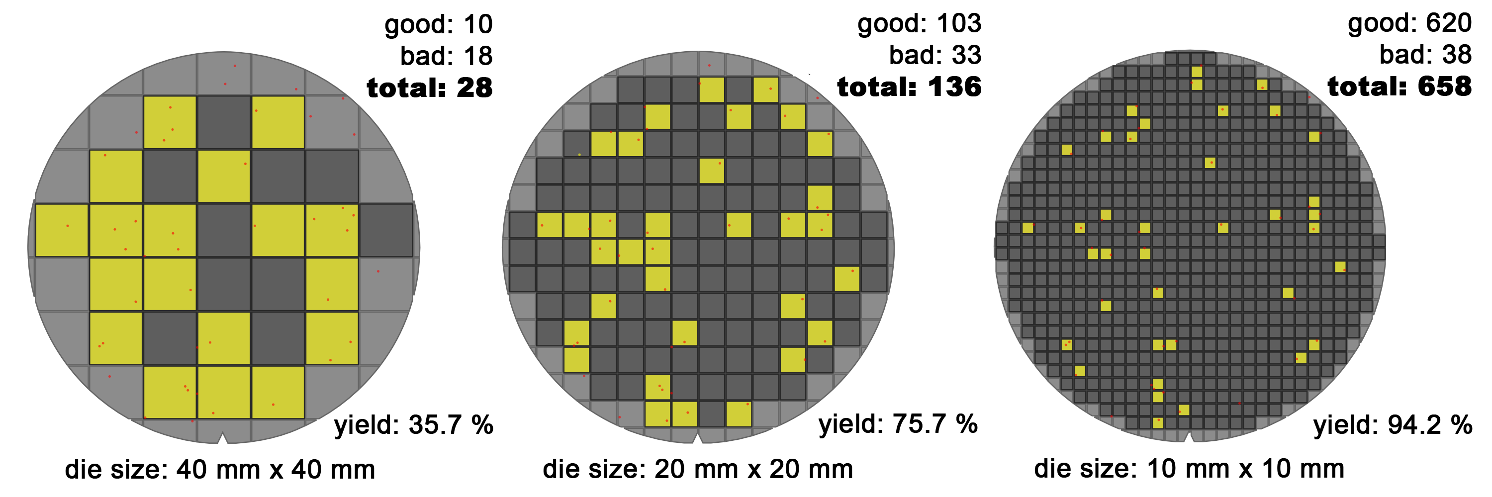
As you can see, each wafer has the exact same number and placement of defects (red dots). Each defect is ruining a higher percentage of each large die simply due to the size of the chip. Thus the larger the die, the lower the yield.
In addition, the larger the die you try to harvest from a wafer the more waste you have. Which also increases your cost:
It is much easier to get good yields from a small chip than a large chip.
Last edited:
AtenRa
Lifer
- Feb 2, 2009
- 14,003
- 3,362
- 136
Wouldn't that just lead to no retail units soon, maybe for the year?
Yes, i believe that we will not see GP100 in desktop market in 2016. NV will most probably produce enough chips to fulfill its CRAY orders and thats it.
TRENDING THREADS
-
 Discussion Zen 5 Speculation (EPYC Turin and Strix Point/Granite Ridge - Ryzen 9000)
- Started by DisEnchantment
- Replies: 25K
-
Discussion Intel Meteor, Arrow, Lunar & Panther Lakes + WCL Discussion Threads
- Started by Tigerick
- Replies: 24K
-
 Discussion Intel current and future Lakes & Rapids thread
- Started by TheF34RChannel
- Replies: 24K
-

-

AnandTech is part of Future plc, an international media group and leading digital publisher. Visit our corporate site.
© Future Publishing Limited Quay House, The Ambury, Bath BA1 1UA. All rights reserved. England and Wales company registration number 2008885.