So I guess new Optane and 300-series chipsets aren't launching today.
I did just listen to Rob Crooke's speech at Morgan Stanley TMT conference. For 3D NAND, he emphasized the role of the technology is foremost achieving most bits/mm2. They seem to be doing that well with the recent SSDs like the 760p, achieving excellent performance at low cost, and low power. For 3D XPoint based products, for this year its mostly about proliferating the products to meet cost targets better, but with the primary goal of improving performance.
Density wise, he was talking about QLC NAND, with greater vertical stacks and even the traditional shrink to do so. With Optane and density it was about increasing the current 2 stack layer into higher ones, and traditional shrink. There were analyzations done that said 3D XPoint gets better with lithography shrink and its metrics improve. Like in performance and durability.
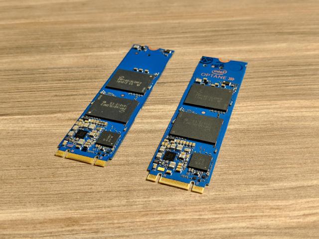
Optane Memory 16GB and 32GB drives internally identify themselves as 800p.
Billy, weren't they called 8000p? The early leaks also had them with higher specs. The write was almost double. And thanks for your thoughts on the matter.
There's a fairly recent PCN that states some PCB size changes for the 800P models. No way to tell why it was done. I'm still of the belief that they'll release it all with 300-series chipsets, because it makes sense.
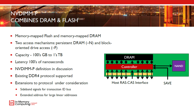
DIMMS reportedly uses 15-18w of power depending on the workload and because of their dimensions require reworked mobos.
I've seen that figure before. I think they'll launch Cascade Lake in early Q3, but announce Apache Pass DIMMs coming later in the year. That allows unnecessary delaying of the platform, without having to risk the DIMMs falling short of expectations because it launched too early. Exciting tech for sure, but lots of hurdles to clear.