
From the other thread:
GP106
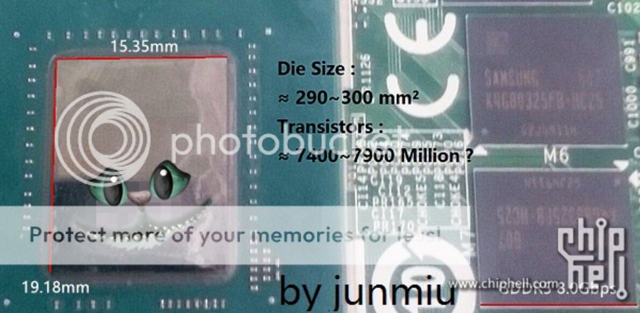
GP104 - ~ 290-300mm²
GP106 - ~195-205mm²
back to topic:
http://www.hardwareluxx.de/index.ph...it-pascal-gpu-und-samsung-gddr5-speicher.html
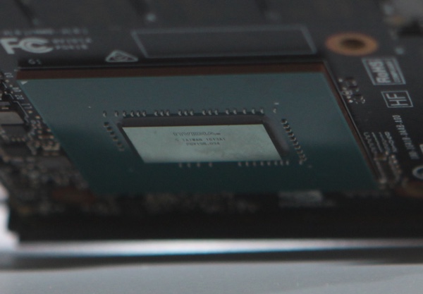
GP106 spotted in Revision A1 (should be the production one) and made in week 13 of 2016 (we are week 15). Still hot from the oven !
For such small chip, qualification should be fast and we can expect to see boards in retail before September.
Then on chiphell forum, someone showed ~300mm² Pascal with 8GB GDDR5 (link doesn't work for me but there is it: https://www.chiphell.com/thread-1563086-1-1.html )
Looks like Nvidia is going to deploy Pascal from top to bottom at very fast pace (this is where deep pockets and big R&D budget helps)
GP 106 should be 180-200mm2 SKU
http://www.hardware.fr/news/14589/gtc-200-mm-petit-gpu-pascal.html
Gp104 350-400mm2
GP106
GP104 - ~ 290-300mm²
GP106 - ~195-205mm²
Last edited:
")