NVIDIA GeForce 20 Series (Volta) to be released later this year - GV100 announced

Page 14 - Seeking answers? Join the AnandTech community: where nearly half-a-million members share solutions and discuss the latest tech.

Ajay

Lifer
Jan 8, 2001
16,094
8,111
136
Breaking news. Fermi core, clock for clock, core per core, performs an ADD or MUL operation at same speed than Volta and even Polaris. But does Fermi offer same performance than Volta ? of course not.
They are no such concept of IPC gain per core in GPU world. Not from Nvidia. Not from AMD. Gains are from moar cores, higher clock speeds and better core utilization.

Great points. An FMADD unit is pretty basic chunk of logic. They were optimized a long time ago (as soon as there were enough xtors to reduce cycle count to something sane).
 

Phynaz

Lifer
Mar 13, 2006
10,140
819
126
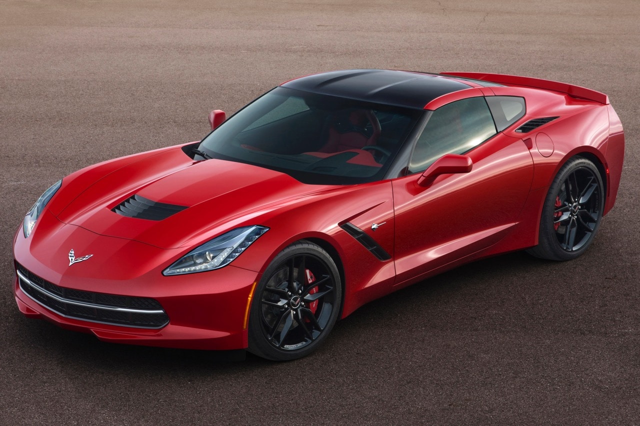
Wow, Volta to Vega is a Chevy Corvette compared to a Chevy Vega.

Going by the number of posts added to this thread in the last 24 hours some people are really upset about Volta's performance.


This is outright trolling. Nearly everyone else is having a somewhat technical discussion and you just come in here and drop a load of dumb on it, spawning a bunch more terribad posts.

AT Moderator ElFenix
 
Last edited by a moderator:
Mar 10, 2006
11,715
2,012
126
Wow, Volta to Vega is a Chevy Corvette compared to a Chevy Vega.

I didn't know what those cars are; for people equally as ignorant about cars as I am, here are some visual aids:

Vega
images


Corvette
2014_chevrolet_corvette-stingray_coupe_z51_fq_oem_1_1280.jpg
[/QUOTE]
 
  • Like
Reactions: psolord and Phynaz

swilli89

Golden Member
Mar 23, 2010
1,558
1,181
136
Comparing a 70's car with a new car.

Would be a more apt description if nvidia's "async computer and DX12 ability" was like if Chevy said you have a GPS Navigation system and instead included a hand paper map with a flash light :p
 

Bouowmx

Golden Member
Nov 13, 2016
1,150
553
146
Car analogies. :neutral: w/e

Concerning GPU "stuff (instructions or performance) per clock", you can look at it theoretically, which has been 2 FLOP/cycle for a long time, not revealing of differences between architectures, or practically, such as core utilization or "FLOPS efficiency", which Maxwell increased over Kepler.
 

Ajay

Lifer
Jan 8, 2001
16,094
8,111
136
Car analogies. :neutral: w/e

Concerning GPU "stuff (instructions or performance) per clock", you can look at it theoretically, which has been 2 FLOP/cycle for a long time, not revealing of differences between architectures, or practically, such as core utilization or "FLOPS efficiency", which Maxwell increased over Kepler.

Yeah, this would be interesting information to have.
 

JoeRambo

Golden Member
Jun 13, 2013
1,814
2,105
136
People are "upset" about a GPGPU card that costs $15,000? I think you just revealed more about yourself than anyone else with that post..

More likely those certain guys can connect the dots?. If NV is getting 40% more SP/DP FLOPs at same wattage, they know very well what will happen when consumer chips without most of DP/tensor cores are released.
 

Carfax83

Diamond Member
Nov 1, 2010
6,841
1,536
136
More likely those certain guys can connect the dots?. If NV is getting 40% more SP/DP FLOPs at same wattage, they know very well what will happen when consumer chips without most of DP/tensor cores are released.

And certain people in this very thread scoffed when I once said that performance per watt was the most crucial aspect for any GPU. Consumers may not care about performance per watt, but it definitely dictates the overall performance characteristics of a GPU.

Unless AMD finds a way to bridge the gap between NVidia and themselves in this crucial metric, then they will NEVER regain the performance crown. You can mark my words.
 

itsmydamnation

Platinum Member
Feb 6, 2011
2,984
3,671
136
More likely those certain guys can connect the dots?. If NV is getting 40% more SP/DP FLOPs at same wattage, they know very well what will happen when consumer chips without most of DP/tensor cores are released.

And certain people in this very thread scoffed when I once said that performance per watt was the most crucial aspect for any GPU. Consumers may not care about performance per watt, but it definitely dictates the overall performance characteristics of a GPU.

Unless AMD finds a way to bridge the gap between NVidia and themselves in this crucial metric, then they will NEVER regain the performance crown. You can mark my words.

Vega get 12.5 TFlop @ 300watt on a significantly smaller GPU (smaller dies are harder to cool), so whats with all the doom and gloom? NV's biggest advantages in gaming has nothing to do with ALU, for a long time (fermi?) they had a front end/geometry setup advantage which got fixed with Polaris. Then since maxwell they have had a very big raster advantage.

Now on raster it "seems" (guy broke his link) that NV confirmed they dont do tile based binning:
It's been confirmed by nVidia that this is only used to exploit locality in the L2 cache, there's no tiling going on
"just" L2 locality so Vega can very well have an advantage in that area vs maxwell. We will have to wait and see what improvements NV make in that area ( im sure they will) but they will probably be closer in performance/power then the current polaris/maxwell gulf.

I see the Typical profits of doom are circling but there is still plenty of wait and see to be done......


edit: i'll just add im talking per clock here
 
Last edited:

raghu78

Diamond Member
Aug 23, 2012
4,093
1,475
136
And certain people in this very thread scoffed when I once said that performance per watt was the most crucial aspect for any GPU. Consumers may not care about performance per watt, but it definitely dictates the overall performance characteristics of a GPU.

Unless AMD finds a way to bridge the gap between NVidia and themselves in this crucial metric, then they will NEVER regain the performance crown. You can mark my words.

Zen and Vega are the first major CPU and GPU design efforts by AMD in half a decade. AMD has proved with Zen they can design a power efficient and competitive CPU core. So there is no reason to doubt that they cannot design a power efficient GPU architecture. Anyway the goal for AMD is to close the efficiency gap with Zen/Vega against Intel and Nvidia and continue to keep doing so. AMD does not need the performance crown. They need power and area efficient architectures (perf/watt and perf/sq mm). Most importantly they require consistently good execution. With competitive CPU and GPU architectures AMD has the unique capability of providing the world's best x86 APUs - something which Intel and Nvidia cannot do . There is one key missing technology which needs some time to be available in volume and at good yield/cost -HBM. HBM2 is just starting to become available but HBM3 and low cost HBM might be the tipping point when AMD's Fusion concept truly delivers to its potential. HPC server APUs, Game console APUs, Notebook / Desktop APUs are all going to need massive bandwidth at 7nm as its a massive process node shrink of almost 60% and extremely powerful GPUs are going to be packed into all these chips. Truly AMD has a bright future. They just need to keep building on the strong foundations they are building today. :)
 

Head1985

Golden Member
Jul 8, 2014
1,867
699
136
Comparing GV100 (5120 cores) to GP100 (3584 cores) we see a 42.8% increase in cuda cores. The FLOP increase is 41.5% from 10.6 to 15.0 TF. Core clocks have fallen only around 1.5% and TDP is still 300W. This is an amazing engineering achievement even if we consider the 33% die size increase from GP100 (610 sq mm) to GV100 (815 sq mm) . Volta is a massive improvement in power efficiency and I guess there are 2 parts to how Nvidia achieved that - architecture and the 12FFN process.

Looking forward to GV102 , GV104 and GV106 we can expect the following

GV102 (5376) - 5120 cc enabled at launch. Performance 40-50% faster than TitanXp. Die size 600 sq mm approx
GV104(3584) - 3584 enabled at launch. Performance 5-10% faster than Titan Xp. Die size 400 sq mm approx
GV106(1792) - 1792 enabled at launch. Performance equal to GTX 1070 or slightly better. Die size 250 sq mm approx.

AMD will have a very tough time in 2018 against this stack. Nvidia could again get to 80+% market share in 2018.
yeah it will be hawaii vs maxwell all over again.
Btw how many SP you expecting in GTX2070?How much it will be cutdown?I expecting 2560SP
 
  • Like
Reactions: psolord

tamz_msc

Diamond Member
Jan 5, 2017
3,865
3,729
136
yeah it will be hawaii vs maxwell all over again.
Btw how many SP you expecting in GTX2070?How much it will be cutdown?I expecting 2560SP
I also think that it will be 2560 CUDA cores, which already brings it to the level of the GTX 1080, and I'm expecting 30 percent additional improvement due to the architectural changes, which would enable it to match the GTX 1080 Ti. This has been the trend in the past - 780 Ti vs 970, 980Ti vs 1070.
 
  • Like
Reactions: psolord

Glo.

Diamond Member
Apr 25, 2015
5,845
4,855
136
It appears that both "brand cheerleading camps" are getting way ahead of ... everything.

The hype on both brands is enormous. Cool it down guys. Interesting times ahead.
 
  • Like
Reactions: Ajay

SpaceBeer

Senior member
Apr 2, 2016
307
100
116
Huang said develpment cost of GV100 was around 3 billion USD (in 3y period). So I suppose nVidia will do their best to maximize profits, ie. sell the smallest chips they can for the highest possible price. Therfore I expect GV 104 will be 350 mm^2 chip, if not even smaller
 

iBoMbY

Member
Nov 23, 2016
175
103
86
Vega 10 really isn't a competitive product to GV100 - that would be Vega 20.

That depends how good the new GFX9 architecture is (how much more of the raw potential can be effectively used). The FP raw performance per Shader Processor is almost equal, and the performance per Watt may even be better on Vega. Vega 10 has only half the memory speed, but will also cost half (or less). Also, how many Wafers do you think it will take to get one working GV100?
 

Qwertilot

Golden Member
Nov 28, 2013
1,604
257
126
Its is more or less absolutely guaranteed that GV2080 will be a little ahead of the 1080ti, 2070 roughly equal etc. Then the big chip a chunk ahead again.

GV100 shows that there's enough technical scope for them do so, so they'll size/specify the details - memory, precisely how much they cut etc - to achieve that. Just what NV do and what they need to do to keep their upgrade train rolling.
 

tamz_msc

Diamond Member
Jan 5, 2017
3,865
3,729
136
Vega get 12.5 TFlop @ 300watt on a significantly smaller GPU (smaller dies are harder to cool), so whats with all the doom and gloom? NV's biggest advantages in gaming has nothing to do with ALU, for a long time (fermi?) they had a front end/geometry setup advantage which got fixed with Polaris. Then since maxwell they have had a very big raster advantage.

Now on raster it "seems" (guy broke his link) that NV confirmed they dont do tile based binning:
"just" L2 locality so Vega can very well have an advantage in that area vs maxwell. We will have to wait and see what improvements NV make in that area ( im sure they will) but they will probably be closer in performance/power then the current polaris/maxwell gulf.

I see the Typical profits of doom are circling but there is still plenty of wait and see to be done......


edit: i'll just add im talking per clock here
The guy updated the link, he could not find the original GDC presentation but linked to a hardware.fr article that covered it in March.
https://translate.googleusercontent...l.html&usg=ALkJrhhwBvlXFiA0Bf7MYl59l0k11JHzjw
 

lobz

Platinum Member
Feb 10, 2017
2,057
2,856
136
Wow, Volta to Vega is a Chevy Corvette compared to a Chevy Vega.

Going by the number of posts added to this thread in the last 24 hours some people are really upset about Volta's performance.
about which we don't know anything
 

jpiniero

Lifer
Oct 1, 2010
15,551
6,026
136
That depends how good the new GFX9 architecture is (how much more of the raw potential can be effectively used). The FP raw performance per Shader Processor is almost equal, and the performance per Watt may even be better on Vega. Vega 10 has only half the memory speed, but will also cost half (or less). Also, how many Wafers do you think it will take to get one working GV100?

It's more about the feature set than anything else. Vega 10 doesn't have DP nor any kind of DL accelerator. Yeah, GV100 is a bit of a kitchen sink approach but apparently that's what Oak Ridge wanted?
 

KompuKare

Golden Member
Jul 28, 2009
1,216
1,566
136
Huang said develpment cost of GV100 was around 3 billion USD (in 3y period). So I suppose nVidia will do their best to maximize profits, ie. sell the smallest chips they can for the highest possible price. Therfore I expect GV 104 will be 350 mm^2 chip, if not even smaller
It's sort of strange how Nvidia like to boast about their cumulative spent, whereas Intel seldom do especially when talking about their cumulative losses trying to break into mobile.
Anyway, these figures are meant to be public so I looked them up:
https://ycharts.com/companies/NVDA/r_and_d_expense
April 2014 to April 2017 has the cumulative spend of $4.56 billion. So if Volta was $3 billion of that, then everything else during that time was only £1.56 billion. That everything else includes losses for mobile, and all their other graphic card research.
 

Cakefish

Member
Oct 10, 2014
156
15
81
www.facebook.com
Now I have to start saving for the upcoming GV104 part that's just around the corner. Crazy how fast the PC GPU market is moving! I haven't even had my 1080 for a year and it's already outdated not only by a higher tier Pascal card (that I was expecting) but by a whole new architecture and process node (this release date took me by surprise).