Multiple dies acting as one on interposer

Page 3 - Seeking answers? Join the AnandTech community: where nearly half-a-million members share solutions and discuss the latest tech.

maddie

Diamond Member
Jul 18, 2010
5,161
5,554
136
You're misunderstanding me. AMD's discomfort with the naming conventions isn't because they have the ability to swap blocks in and out of chips, but because around the same basic compute unit version they might have different IP blocks and so "GCN1.2" chips might not be homogeneous in their feature set. The example given is that while Tonga and Fiji are both GCN1.2 (or GCN3), one has HVEC while the other doesn't. It's the extending of the CU version to cover the whole chip that is the problem. While AMD definitely does have the ability to match GCN1, 2 , etc CUs with different other blocks, the next sentence saying they don't have to redesign to whole GPU to modify part of it is a pretty big simplification.

Yes, they're separate IP. You could mix and match GCN CU's from different versions, different other features, say leave off a XDMA from a low end part, etc while building a new chip. That doesn't necessarily mean that you can do something like grab the new MC and L2 from Polaris, quickly toss it on a respin of Hawaii, and sell that into the midrange market. Maybe you could back port it, or say update Hawaii with HVEC and HDMI2.0, but that doesn't mean it'd be a quick job.
Let me ask these questions.

If they are designing a new GPU, do you think they can place these different IP blocks on separate die if you can connect these separate die through the interposer just as easily as through the traditional on die connections?
Will it be more difficult to do it this way [multi-die] if the connecting pathways are available and comparable for both options?
 

MrTeal

Diamond Member
Dec 7, 2003
3,919
2,708
136
Let me ask these questions.

If they are designing a new GPU, do you think they can place these different IP blocks on separate die if you can connect these separate die through the interposer just as easily as through the traditional on die connections?
Will it be more difficult to do it this way [multi-die] if the connecting pathways are available and comparable for both options?

Yes, I would imagine it would be, though I'm hardly the person to ask. My chip layout experience consists of making a basic ALU in Cadence Virtuoso at 130nm during university.

Some things like a PCIe PHY, XDMA engines, maybe not so much. Big wide busses like what appears to be between the L1 and GDS, the L2s and the crossbar to the CUs, the memory controllers and all the render backends won't necessarily be as easy. Keep in mind you have a bunch of metal layers on a chip, and they tend to come (after M1) in groups based on the rules. Metal 2-5 might have certain pitch/area rules, 6-7 another, etc. The trend is that outer metal has a bigger pitch than the inner metal layers. I have no idea how any of the internally laid out and routed (and I doubt anyone outside AMD or the foundries does, unless it's in one of the Chipworks reports), but if you are having big wide buses that have to be popped out of the middle of the metal stack to the top layer and bumped before running elsewhere, I can see how that would affect not only your existing layout, but the capacitance and drive required.

Again, not that I don't think this could be done even with GPUs though inter-GPU communication is going to be different than even a many core processor as described in the paper. It's not even like it's a bad idea. I just don't think adapting an architecture like GCN that while scalable is still designed for a monolithic die is anything resembling a simple task. If AMD is pursuing this, and it wouldn't surprise me at all if they were, I would imagine it would a small group moving from theoretical simulations and papers to physical proof of concepts on old and cheap nodes, at which point they can look at redesigning their graphics core from the ground up to be scalable in this way.
 

maddie

Diamond Member
Jul 18, 2010
5,161
5,554
136
Yes, I would imagine it would be, though I'm hardly the person to ask. My chip layout experience consists of making a basic ALU in Cadence Virtuoso at 130nm during university.

Some things like a PCIe PHY, XDMA engines, maybe not so much. Big wide busses like what appears to be between the L1 and GDS, the L2s and the crossbar to the CUs, the memory controllers and all the render backends won't necessarily be as easy. Keep in mind you have a bunch of metal layers on a chip, and they tend to come (after M1) in groups based on the rules. Metal 2-5 might have certain pitch/area rules, 6-7 another, etc. The trend is that outer metal has a bigger pitch than the inner metal layers. I have no idea how any of the internally laid out and routed (and I doubt anyone outside AMD or the foundries does, unless it's in one of the Chipworks reports), but if you are having big wide buses that have to be popped out of the middle of the metal stack to the top layer and bumped before running elsewhere, I can see how that would affect not only your existing layout, but the capacitance and drive required.

Again, not that I don't think this could be done even with GPUs though inter-GPU communication is going to be different than even a many core processor as described in the paper. It's not even like it's a bad idea. I just don't think adapting an architecture like GCN that while scalable is still designed for a monolithic die is anything resembling a simple task. If AMD is pursuing this, and it wouldn't surprise me at all if they were, I would imagine it would a small group moving from theoretical simulations and papers to physical proof of concepts on old and cheap nodes, at which point they can look at redesigning their graphics core from the ground up to be scalable in this way.
Is this what you are referring to?


Slide%209%20-%20Power%20Frequency%20curve%20with%20libraries.png
 

MrTeal

Diamond Member
Dec 7, 2003
3,919
2,708
136
Is this what you are referring to?

Essentially, yeah. That's actually kind of funny, I think that's an image of an Intel stack on the AMD slide. The CPU centric slide is a little different than you might normally see in a GPU where the design rules might be more bunched, but then none of these guys really follow design rules anyway, especially not on a four year old process.
Carrizo uses an interesting stackup, they have 8 M1 layers, then one 2x and one 4x, and finally two x16 layers on top. From my understanding Fiji uses 11 metal layers, but I have no idea how they are arranged.

I can't wait to see (if I can find the info) what early 14nm looks like. I suspect they won't get the upper layer density until they familiarize themselves with the process.

Edit: this gives you a good view of a few different metal stacks.
bgbsja.png
 
Last edited:

Mr Evil

Senior member
Jul 24, 2015
464
187
116
mrevil.asvachin.com
Could this make compound semiconductors more feasible? One of the reasons why the more interesting non-silicon technologies like GaInAs haven't seen much use is because they are hard to grow on a silicon substrate. If you could attach a GaInAs chip to a silicon interposer, then that would no longer be a problem. Maybe you could mix in completely different materials like graphene too, using the optimal material for each part of the GPU.
 

Paul98

Diamond Member
Jan 31, 2010
3,732
199
106
Yeah it does allow you to use totally different parts or nodes on the interposer.
 

JDG1980

Golden Member
Jul 18, 2013
1,663
570
136
The NVIDIA GeForce GTX 660 Review: GK106 Fills Out The Kepler Family

In the intervening time, the lineup was filled with Fermi. The GTX 570 provided 85% of the $300 660 Ti's performance at $250, and the 560 Ti provided 67% of it at closer to $200. Hell, the 550Ti was still available at $119 vs the $109 of the GK107-based GT 640, and it was way, way faster than the 640.

If P10 is ~100mm² and P11 is ~300mm², I'd expect them to continue to sell existing 28nm designs in the missing price points.

I think that mixing any 28nm products into AMD's new lineup would be a mistake. At a minimum, the 400-series designation (or whatever other new designation AMD/RTG wants to use for the new generation) shouldn't be watered down by including 28nm products, just as the 7000 series was exclusive to GCN (except a handful of OEM-only trash on the ultra-low-end).

One possibility is that AMD could fill the midrange with salvage dies until midsize Polaris is ready. After all, yields on big Polaris will likely be quite low at first (has any of the foundries even released a >200mm^2 FinFET chip yet, let alone >300?) Nvidia had three tiers of GK104 near the beginning of 28nm (680, 670, 660Ti). And even with GM204 on a fully mature 28nm process that must have very high yields, we've got 980 and 970 on the desktop side and 980M and 970M on the mobile side. These have shader counts ranging from 2048 for 980 desktop to just 1280 for 970M mobile. If Nvidia is willing to sell a part with 37.5% of its shaders disabled on 28nm now, why wouldn't AMD be willing to do something similar on FinFET at the start?
 

MrTeal

Diamond Member
Dec 7, 2003
3,919
2,708
136
I think that mixing any 28nm products into AMD's new lineup would be a mistake. At a minimum, the 400-series designation (or whatever other new designation AMD/RTG wants to use for the new generation) shouldn't be watered down by including 28nm products, just as the 7000 series was exclusive to GCN (except a handful of OEM-only trash on the ultra-low-end).

One possibility is that AMD could fill the midrange with salvage dies until midsize Polaris is ready. After all, yields on big Polaris will likely be quite low at first (has any of the foundries even released a >200mm^2 FinFET chip yet, let alone >300?) Nvidia had three tiers of GK104 near the beginning of 28nm (680, 670, 660Ti). And even with GM204 on a fully mature 28nm process that must have very high yields, we've got 980 and 970 on the desktop side and 980M and 970M on the mobile side. These have shader counts ranging from 2048 for 980 desktop to just 1280 for 970M mobile. If Nvidia is willing to sell a part with 37.5% of its shaders disabled on 28nm now, why wouldn't AMD be willing to do something similar on FinFET at the start?

They don't have to mix them into the new lineup. They just don't need to draw down supplies on the GPUs that would fit well as quickly. You don't necessarily have to rebrand them, though OEMs might prefer that.

Looking back to the launch of Kepler and 28nm, nVidia had three dies, but the 660Ti still sold for $300. Below that there was nothing, unless you wanted a 640 for your HTPC. If AMD launches P11 at say $550, cut 1 might be $400 and cut 2 might be $300. If P10 really is intended to push hard into mobile and is 950/960 class, you're still going to have a decent gap there even if AMD charges $200 for a P10 card.
 

boozzer

Golden Member
Jan 12, 2012
1,549
18
81
Yes.Paper in link in 1# talks of building 64 core CPU using same approach.
ok, I am now excited beyond reason. this needs to happen 1000% :thumbsup::thumbsup::thumbsup:

64 cores acting as one core!!!!!!!!!!!!!!!!!!!!!!!!!!!!!!!!!!!!!!!!!!!!!! give me!!!!!!!!!!!!!!!!!!!!!!!!!!!
 

maddie

Diamond Member
Jul 18, 2010
5,161
5,554
136
ok, I am now excited beyond reason. this needs to happen 1000% :thumbsup::thumbsup::thumbsup:

64 cores acting as one core!!!!!!!!!!!!!!!!!!!!!!!!!!!!!!!!!!!!!!!!!!!!!! give me!!!!!!!!!!!!!!!!!!!!!!!!!!!
If serious, then sorry to disappoint. The 64 cores are exactly what it says, a 64 CPU unit. The only difference is it being reassembled using smaller core count blocks by using an interposer vs a monolithic approach.
Having said that, the benefits are real.
 

maddie

Diamond Member
Jul 18, 2010
5,161
5,554
136
Essentially, yeah. That's actually kind of funny, I think that's an image of an Intel stack on the AMD slide. The CPU centric slide is a little different than you might normally see in a GPU where the design rules might be more bunched, but then none of these guys really follow design rules anyway, especially not on a four year old process.
Carrizo uses an interesting stackup, they have 8 M1 layers, then one 2x and one 4x, and finally two x16 layers on top. From my understanding Fiji uses 11 metal layers, but I have no idea how they are arranged.

I can't wait to see (if I can find the info) what early 14nm looks like. I suspect they won't get the upper layer density until they familiarize themselves with the process.

Edit: this gives you a good view of a few different metal stacks.
bgbsja.png
I see in the samples provided that all have varying metal layers. but Carrizo has all uniform. Access should be simpler with this.
 

boozzer

Golden Member
Jan 12, 2012
1,549
18
81
If serious, then sorry to disappoint. The 64 cores are exactly what it says, a 64 CPU unit. The only difference is it being reassembled using smaller core count blocks by using an interposer vs a monolithic approach.
Having said that, the benefits are real.
my original question was basically asking if the tech works with cpu, and it does. how come the 64 cpus will still act as individual cores? I thought the interposer connects them all? something akin to super computers.
 

hrga225

Member
Jan 15, 2016
81
6
11
my original question was basically asking if the tech works with cpu, and it does. how come the 64 cpus will still act as individual cores? I thought the interposer connects them all? something akin to super computers.

Yes,you have few dies, (e.g. 4 with 16 core each;can be any other number) you connect them and basically have one big MULTICORE (64 -core) processor.
He answered you that way,because your post sounded like you are exited about having one ultra wide SINGLE core.
 

Erenhardt

Diamond Member
Dec 1, 2012
3,251
105
101
Interposer HBM apu will be a ground breaking product. A different approach to a socket entirely. It will open many possibilities. Can't wait to see where the tech is going!
 

hrga225

Member
Jan 15, 2016
81
6
11
Again, not that I don't think this could be done even with GPUs though inter-GPU communication is going to be different than even a many core processor as described in the paper. It's not even like it's a bad idea. I just don't think adapting an architecture like GCN that while scalable is still designed for a monolithic die is anything resembling a simple task. If AMD is pursuing this, and it wouldn't surprise me at all if they were, I would imagine it would a small group moving from theoretical simulations and papers to physical proof of concepts on old and cheap nodes, at which point they can look at redesigning their graphics core from the ground up to be scalable in this way.

That is why I have put date of introduction to market so far out.Good points.

Now,I do think that many of hurdles are resolved,though many still need to be resolved,and companies involved are keeping it very low key,for obvious reasons.I also cannot find any downsides of pursuing this research.As chip companies move to smaller nodes they will need things like higher bandwidth,better interconnects etc. because they will be dealing with things like how to feed 50 billion,yes 50 billion,transistor monster.
 
Last edited:

boozzer

Golden Member
Jan 12, 2012
1,549
18
81
Yes,you have few dies, (e.g. 4 with 16 core each;can be any other number) you connect them and basically have one big MULTICORE (64 -core) processor.
He answered you that way,because your post sounded like you are exited about having one ultra wide SINGLE core.
I don't care how many cores there are in the die physically, as long as they act as a single core (software wise). or 16 cores x 4 would work too :)
 

Techhog

Platinum Member
Sep 11, 2013
2,834
2
26
I don't care how many cores there are in the die physically, as long as they act as a single core (software wise). or 16 cores x 4 would work too :)

That's not what anybody is talking about. I don't know how you even got this idea.
 

maddie

Diamond Member
Jul 18, 2010
5,161
5,554
136
I don't care how many cores there are in the die physically, as long as they act as a single core (software wise). or 16 cores x 4 would work too :)
The only work I know about that will accomplish this is from this company.
Interestingly, 3 of the 7 investors on the main page is AMD, Samsung and GlobalFoundries.

I believe the first products will be available this year. [meaning commercial]

http://www.softmachines.com/about/

Working silicon has already been displayed to investors. I guess there must be some merit to raise Million $175.
 
Last edited:

MrTeal

Diamond Member
Dec 7, 2003
3,919
2,708
136
I don't care how many cores there are in the die physically, as long as they act as a single core (software wise). or 16 cores x 4 would work too :)

That's not what the interposer does. Even today an octo-core i7-5960X or AMD FX chip are eight cores on the same die, but they aren't functionally a single core to software. The interposer just lets you put more cores on different dies, but treat them like multiple cores on the same die.
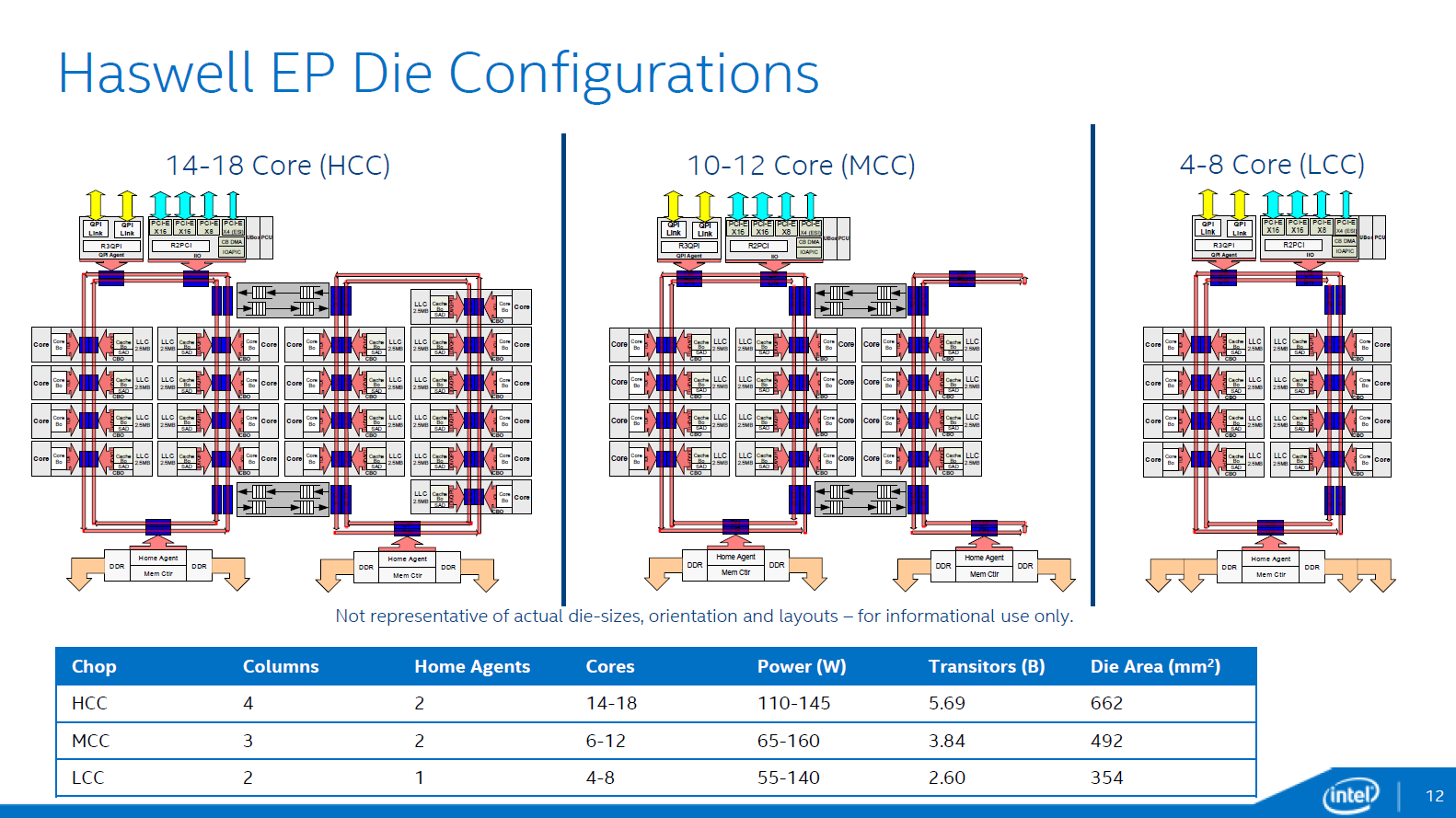
IE:
HaswellEP_DieConfig.png

Haswell-EP HCC is a massive 662mm² die, while the eight core LCC is 354mm².

Let's pretend they used an interposer here (ignoring size issues of needing a bigger socket), Intel could have created a single 8 core die with a ring bus, PCI-e/QPI subsystem, and Home Agent/quad channel Memory controller, along with the logic and queues for the buffered switch. Essentially it'd be a version of LLC plus the switch logic.

For a single die, you'd sell it as is for the current Haswell-E and Xeon 4-8 core lineup. From there, you could put two of these together and fuse off the PCIe and two of the channels to make a 16 core die. If you wanted to go really extreme, you could go with an even bigger socket and have a 32 core, octo channel memory part. There's obviously downsides to doing that, but it would be interesting and relatively lower effort in my opinion. We're just getting Broadwell-E soon, and it might be even longer before we see the 22 core die. On the switch to 10nm, it might be a way to produce very large core counts early in the node as maddie likes to advocate. Of course, Intel just charges $5000 for one of the big dies, so you can suffer pretty low yields before that becomes unprofitable. :p
 
Last edited:

maddie

Diamond Member
Jul 18, 2010
5,161
5,554
136
So far we have been mostly talking about the merits and pitfalls of
technical, performance and production costs factors.

Can anyone give some feedback on stock management, ability to quickly vary production of the product mix within the range?

I would imagine a faster response time to changes in segment sales [die on hand can be used for different product segments]and a lower overall inventory cost [no need to stock various die].
 

boozzer

Golden Member
Jan 12, 2012
1,549
18
81
That's not what the interposer does. Even today an octo-core i7-5960X or AMD FX chip are eight cores on the same die, but they aren't functionally a single core to software. The interposer just lets you put more cores on different dies, but treat them like multiple cores on the same die.
IE:
HaswellEP_DieConfig.png

Haswell-EP HCC is a massive 662mm² die, while the eight core LCC is 354mm².

Let's pretend they used an interposer here (ignoring size issues of needing a bigger socket), Intel could have created a single 8 core die with a ring bus, PCI-e/QPI subsystem, and Home Agent/quad channel Memory controller, along with the logic and queues for the buffered switch. Essentially it'd be a version of LLC plus the switch logic.

For a single die, you'd sell it as is for the current Haswell-E and Xeon 4-8 core lineup. From there, you could put two of these together and fuse off the PCIe and two of the channels to make a 16 core die. If you wanted to go really extreme, you could go with an even bigger socket and have a 32 core, octo channel memory part. There's obviously downsides to doing that, but it would be interesting and relatively lower effort in my opinion. We're just getting Broadwell-E soon, and it might be even longer before we see the 22 core die. On the switch to 10nm, it might be a way to produce very large core counts early in the node as maddie likes to advocate. Of course, Intel just charges $5000 for one of the big dies, so you can suffer pretty low yields before that becomes unprofitable. :p
I am sad, my dreams shattered. IF coding for 8 cores or more is as hard as it is right now, I can't imagine a reasonable adoption rate for more cores. I can obvious see the uses for business/commercial but nothing on the consumer side which is what I care about. :'( damn
 

hrga225

Member
Jan 15, 2016
81
6
11
I am sad, my dreams shattered. IF coding for 8 cores or more is as hard as it is right now, I can't imagine a reasonable adoption rate for more cores. I can obvious see the uses for business/commercial but nothing on the consumer side which is what I care about. :'( damn
Let's take bulldozer core.It is pretty narrow,2 int and 2 agu alu,so 4 int pipes.If you combine them the way you thought you would have 256 int pipe wide core.
Just out of curiosity, what workload would you run on such a core?
 

boozzer

Golden Member
Jan 12, 2012
1,549
18
81
Let's take bulldozer core.It is pretty narrow,2 int and 2 agu alu,so 4 int pipes.If you combine them the way you thought you would have 256 int pipe wide core.
Just out of curiosity, what workload would you run on such a core?
I am not sure what your question pertains to, I will list what I use my computer for. gaming, light video editing, adobe lightroom. also have a bad habit of having 10+ programs open most of the time. as tech enthusiast. I just like shiny new tech, before the stagnation of tech in the last 5 years, I used to upgrade almost every year.