Lol. Poor choice of words then, are there any updates to their eyefinity technology?
Supposedly yes. Dubbed "Eyefinity +", Eyefinity 4, Eyefinity+.... The rumours are: No more requirement for Dispayport combined with an active DP->DVI adapter. The cards also now have 5 outputs instead of 4. 2x DVI, HDMI, 2x Mini-DP. Instead of one DP like on Evergreen, there are now two Mini-DP on NI. Supposedly now you can run higher resolutions without the need of an active adapter (which you cannot do on Evergreen). Then theres the rumor of support for super ridiculous HD resolutions - like 20 or 30 megapixel or something. And triple monitor on dvi+dvi+hdmi might be possible (also not possible on Evergreen). And as the name implies - four screen eyefinity support in the drivers. The 4 screen layouts were said to be supported at the launch of eyefinity Sept 2009, however I didn't see too many people actually running it.
I guess it would be 3x1 gaming setup in landscape or portrait orientation, with a 4th display on the top or side running windows apps or maybe even a game console or menu.
IMO, AMD really needs a "BIG BANG" style re-do of their CCC and drivers with better stability, compatibility & performance. They could make an entire press release over just that by itself. But Kudos to them for really pushing the hardware envelope, no matter how gimmicky and bug-ridden it seems to be.
Anyways...
Everyones talking about how this "is a minor refresh" or is "a gpu redesign" etc. Even some of these "news articles" make me sick. But it's just a bunch of dumb arguing without data to validate points & opinions. IMO it's more similar to GT200->GF100 than G80->G92. G80->G92's greatest difference was the shrink. GT200->GF100 was the complete redesign to the "FERMI" mArch.
RV770-> Cypress was a shrink, and a doubling of ALU power, and a redesigned Ultra threaded dispatcher & Scheduler. In my eyes that's pretty similar to G80->G92; the differences being where Nvidia shrank the trace halls, Ati stayed at the same node and doubled up everything. Overall the changes in principle design weren't drastic by either company, but the performance impact was good and the dies were small, impressive, sold well, & were popular because of their aggressive pricing and high yield.
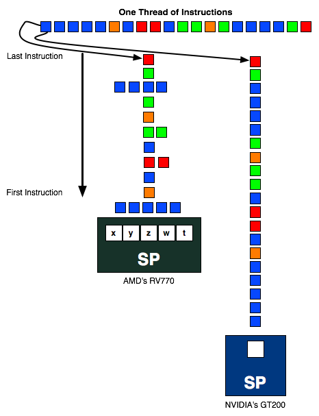
Since R600 AMD has used a Stream Proccessor (Unified pixel processor, Vertex processor, Shader, TP, SP, SPU, Core, CC, Cuda core, w-t-f-y-w-t-c-i) that is like Nvidia's cuda core, except broken into 5 slots or parts or lanes (5-way, 5-wide, 4+1). IFIRC: it's the w,x,y,z, and t-unit. I don't know too much about the details, but each of the 5 slots can take instructions running down the pipeline when said instruction is compatible with said slot. The benefit is to break down the instruction sending more parts of it into the shader, getting the work done quicker. BAM - a shader that can do more, quicker, in the same space. AMD must have considered this so impressive that instead of calling the arithmetic logic unit a core or shader, they called each of the 5 parts a shader. Now you get 5 for the price of 1 - great for the marketing department. "Now instead of 160 shaders, we have 800, suckers." So that's why there are huge inflated numbers for shader count on AMD cards... like 1,600. Nvidia's GTX480 has 480 shaders (CUDA CORES TM). AMD's HD5870 has 1600 shaders - but it's really more like (1600/5) if you were to make a direct comparison to one of Nvidia's shaders. So that would leave the HD5870 with 320 'actual' cores that are divided into 5 different parts (aka the 5-way Vec5 super-scalar nomenclature). That design was present in the HD2900xt, 3870, 4870, 5870, and maybe even earlier than that - I don't even know. I think they copied the pixel processor + vertex processor 'Unified shader & driver model' bs created by Nvidia in the G80. Anyways, come october 12, when Anand writes his Northern Islands article, we will see that ALU (AMD's Vector 5-way superscalar blah-blah) morphed into something a lil' different.
Now the rumour is that AMD has redesigned that 5-way shader. Instead of 5 slots, they are going with 4. 5 slots ended up being like 70-80% efficient. The instruction would come in, and the scheduler, uncore, bs whateva would chop it up, trying to fill the slots - like a road cone or traffic cop. (kind of like when multiple lanes of traffic approach a toll both and line up in 5 lanes at 5 booths).
Take this analogy and imagine that only 18-wheelers can use the 5th booth. However, there is only an 18-wheeler passing through this toll-way every 5 mins or so, while there are regular passenger vehicles passing through by the 1000's per minute. So 4 of the 5 booths are at peak efficiency with passenger cars lined up in front of them constantly, while the 5th booth has an 18-wheeler passing through it every couple minutes or so. The 18-wheeler cant pass through booths 1-4, and likewise, the passenger cars can't use the 5th booth. That's an Evergreen shader.
Traffic lined up approaching an Nvidia toll booth and an Ati toll booth:
Ati has 5 lanes, and Nvidia a single lane. (One thread of instructions = line of vehicles in traffic)
Now imagine the rumored Northern Islands design where they took booths 1 and 2 and redid them, lanes are wider, can handle more throughput and are overall more efficient. Lane 4 was scrapped and renamed Lane 5. (hope i'm getting this right - for more info visit beyond3d or 3d-center, or someone here can correct me) 18-wheelers and passenger cars can both pass through that lane which was 4 & 5 incorporated. Now, the Toll booth is a bit smaller in actual physical size, a couple of the lanes are wider, and the same amount of traffic (just about) can pass through the toll. They've saved space and are overall more efficient. (no more 5th lane sitting there going unused all the time.) Now this 4-lane design stays used all the time, and there isn't space going to waste. Space is the limiting factor in the design of the gpu... the engineers don't want to waste any die area.
Old toll booth (hd2900xt, 3870, 3870x2, 4870, 4890, 4770, x2300 mobility, 5970, 5870, Juniper, etc etc etc):
New toll booth (rumored to be in 6770, 6850, 6870, barts, antilles, cayman):
Now just like this freakin' toll booth analogy i just created, the Evergreen shader was the old 5 lane booth, and the N. Islands shader is the newly constructed 4 lane booth. It's more efficient, and while the 5-lane booth can pass 10,000 cars per hour, the 4-lane booth accepts slightly fewer- 9,850 cars per hour while using ~80% of the physical footprint. It's a more efficient shader design.
Theres supposed to be a new eyefinity, UVD3 (ati's gpu video decoder), new shader model, refined 40nm design with greater power efficiency, all kinds of advanced changes go along with that redesigned shader. Then the package resides on a more heavy duty thicker PCB. They've changed the voltage regulators buck controllers and masters from Volterra brand to Chil (Same brand on the 480 pcb). The reference designed board is said to have more phases of power and come with a vapor chamber cooler - that's just on the freakin 6770. (Blows my mind that they can create incredible hardware like this and then ship it out being powered by the abortion 'CCC' - But hey, that's what RadeonPro is for, right?) The TDP should go up, even though they are touting impressive power consumption and improvements in energy efficiency. If TDP goes down when die size goes up, then that'll be news to me.
psst - one more thing about the 6770 - it's supposed to have relatively low clocks ~700mhz... might be the card to get for over-clocking on a budget. Then there's a rumor of Cayman being either 256bit or 384bit. Then they are tripling or quadding up on the tessellation power. The little rinkydink capacity of the tessellator in Cypress has been quadrupled in NI. That Unigine benchmark (be it real or fake) shows NI having similar tessellating power comparable to Fermi, whereas Fermi can obliterate Evergreen when benching with extreme tessellation. Remember how excited nvidia was when they showed GF100 running Heaven?
")
With all these changes rumored to be in the works, how can any fud site report their opinion and state it as fact... lol *shakes head*.
It's much more complicated than this, but this is my understanding of AMD's shader design &
rumored Northern Islands redesign. Considering that this 'SHADER' is what is rumored to change in Northern Islands, and it's structure hasn't changed since the freakin 2900xt or earlier, this HAS TO BE A MAJOR redesign. How any dumb news site can write an article speculating about the 6990 and then give their opinion about the architecture and call it a major/minor change is ludicrous. If anyone wants to correct me about what I wrote above (like bryan1995 does and is usually right about it) or expound on it, feel free. For ppl like Ocguy or Keys who would rightfully request a source for info when someone is flapping their jaws - I got most of this from Chiphell, Beyond3d and 3d-Center forums. I'm not trying to BS anyone about anything, this is just my layman's interpretation of the rumors, could be right, could be wrong. Kenny Powers, out.