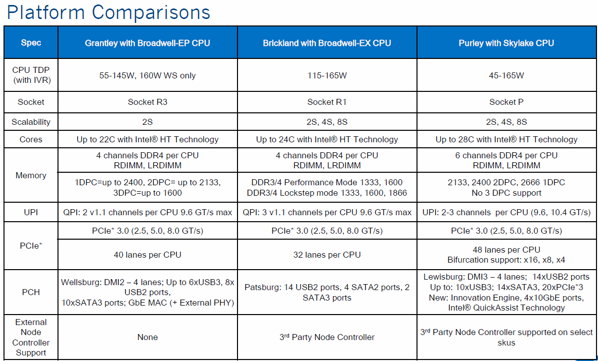
ITT: We speculate on Skylake E5 and E7 Core counts, memory channels, SATA ports, etc

Page 3 - Seeking answers? Join the AnandTech community: where nearly half-a-million members share solutions and discuss the latest tech.

cbn

Lifer
Mar 27, 2009
12,968
221
106
http://www.fool.com/investing/gener...oration-a-look-at-the-new-xeon-d-process.aspx

According to Intel, the Broadwell-U 2+3 configuration features 1.9 billion transistors and fits into an area of 133 square millimeters. This implies a density of approximately 14.3 million transistors per millimeter squared.

SemiAccurate reported that the Xeon D die weighs in at 160 square millimeters. Intel, in a recent post on Twitter, said its Xeon D processor is made up of 4.3 billion transistors -- implying a transistor density of approximately 26.88 million transistors per square millimeter.

But with that big empty spot on the GT3 can we even entertain the idea of a density comparison between these two chips? Furthermore, like Ashraf mentions Xeon-D has 3x more L3 cache which is denser than other forms of logic on a processor die.
 

IntelUser2000

Elite Member
Oct 14, 2003
8,686
3,787
136
Another thing about the Xeon D.

It has 1.5MB L3 cache per core. It sounds similar to how Iris Pro based chips are. The Iris Pro based chips have 1.5MB L3 cache per core because 0.5MB L3 cache is used as tag RAM for the eDRAM cache.

It's possible that Xeon D has physical 2MB L3 cache per core but its using 0.5MB for something else.

I bet they are hiding the actual die picture for competitive reasons.

But with that big empty spot on the GT3 can we even entertain the idea of a density comparison between these two chips? Furthermore, like Ashraf mentions Xeon-D has 3x more L3 cache which is denser than other forms of logic on a processor die.
We don't know what that is.

Also, the extra 8MB L3 cache takes ~400 million more transistors. Even if we assume there's actual 16MB L3 cache, not 12MB that's extra 600 million transistors. Not enough to account for the difference.
 
Last edited:

cbn

Lifer
Mar 27, 2009
12,968
221
106
Here are are the core sizes I came up using the following two pictures:

GT3 Broadwell core size (with empty space included): 8.58 mm2
GT3 Broadwell core size (without empty space): 6.93 mm2

GT2 Broadwell core size: 6.93 mm2

Intel-Broadwell-U-Iris-1024x581.jpg


2%20-%20Die_575px.png
 
Mar 10, 2006
11,715
2,012
126
Not in any meaningful way. DDR3 is basically a full subset of DDR4. The primary differences are in timing parameters and a couple more command options/restriction for DDR4 vs DDR3. Complete noise area wise at best, realistically zero difference.

Pardon my ignorance, but does the same hold true for LPDDR3/4?
 

IntelUser2000

Elite Member
Oct 14, 2003
8,686
3,787
136
Here are are the core sizes I came up using the following two pictures:

GT3 Broadwell core size (with empty space included): 8.58 mm2
GT3 Broadwell core size (without empty space): 6.93 mm2

GT2 Broadwell core size: 6.93 mm2

Technically, that "empty spot" is likely something they hidden it for purpose. It has same pattern as the hidden spots on the cores and graphics. The known empty spot is the left side of the memory controller I/O and it looks much "cleaner". You can see it also with Haswell and Ivy Bridge.

Intel will be presenting a paper on Xeon D at HotChips. I'm crossing my fingers for a die shot.

That's nice. I still think its due to competitive reasons otherwise they'd have plastered the shots everywhere on the internet like they do with other releases.
 
Mar 10, 2006
11,715
2,012
126
Technically, that "empty spot" is likely something they hidden it for purpose. It has same pattern as the hidden spots on the cores and graphics. The known empty spot is the left side of the memory controller I/O and it looks much "cleaner". You can see it also with Haswell and Ivy Bridge.


That's nice. I still think its due to competitive reasons otherwise they'd have plastered the shots everywhere on the internet like they do with other releases.

I don't think so...any of Intel's competitors could buy a Xeon D and tear it down.
 

cbn

Lifer
Mar 27, 2009
12,968
221
106
The known empty spot is the left side of the memory controller I/O and it looks much "cleaner". You can see it also with Haswell and Ivy Bridge.

Yes, as you demonstrated in the link below that dead space/empty spot to the left of the memory controller allows for chop lines to make different die layouts:

http://forums.anandtech.com/showthread.php?t=2234017

But then why is Intel boxing in (ie, including) the "dead space" as part of the memory controller in the GT3 die shot below:

Intel-Broadwell-U-Iris-1024x581.jpg


This compared to the smaller area for the memory controller in the GT2 die below:

2%20-%20Die_575px.png
 
Last edited:

cbn

Lifer
Mar 27, 2009
12,968
221
106
At this point my thinking is that the Broadwell cores in the GT2 and GT3 dies are in fact the same size. (ie, 6.9 mm2 each (without L3 cache)).

...And that something about the GT3 iGPU needs extra xtors forcing Intel to include extra space above the cores and System agent compared to GT2. Maybe this has to do with the connection to EDRAM on the upcoming Broadwell quad core GT3 (or something else required on the iGPU due to having 48 EUs compared to having just 24 EUs)
 

IntelUser2000

Elite Member
Oct 14, 2003
8,686
3,787
136
According to the latest post by Ashraf, the Broadwell Xeon indeed has 24 cores. That's in line with my prediction.

Think about it:

4 to 6
6 to 8
8 to 12
12 to 18*

*Haswell Xeons probably ended up having 18 rather than the logical 16 because they lost some frequency due to unexpected results or plans changed.

That meant Broadwell goes from 18 to 24(or you could call it 16 to 24).

Logically Skylake should be 24 to 32.**

**Really starting to doubt they'll put 32 Skylake cores. Hoping we'll see something new, like Hetereogenous cores or accelerators.
 

tenks

Senior member
Apr 26, 2007
287
0
0
Not trying to be a jerk here, but I think you're honestly all on crack if you think Skylake-EX will have 40 cores. From 18 to 40 in 2 gens? With Intel? ya, no. they're not that generous.
 

ShintaiDK

Lifer
Apr 22, 2012
20,378
146
106
Not trying to be a jerk here, but I think you're honestly all on crack if you think Skylake-EX will have 40 cores. From 18 to 40 in 2 gens? With Intel? ya, no. they're not that generous.

Its not about being "generous". But about reality.

But yes, 40C aint gonna happen on 14nm with Core.
 

Ajay

Lifer
Jan 8, 2001
16,094
8,115
136
Fantastic find mikk! "The biggest platform advancement since Nehalem" almost sounds like an understatement!
 

tenks

Senior member
Apr 26, 2007
287
0
0
Told you! It didn't even crack 30 cores, ha! I was going to make a guess, but even I'm surprised at this low of an increase, lol. 40+ skylake cores on 1 chip, in your dreams.


this also confirms Skylake-E will likely not hit until 2017, especially since it doesn't looked like Broadwell-EP/EX is NOT being skipped, which in turn means we're still getting a late broadwell-e inq1 2016..

I don't know it I can wait till 2017 for skylake-e...sigh

Rnd2MkA.jpg


edit: just caught this. Looks like Intel still refers to the Xeon Phi series as Larrabee internally. Look at the 2S diagram slide where one of the cores is connected to a block via DMI called "LBG". LBG = Larrabee Graphics.


woo I miss the good ole days of news!
 
Last edited:

mikk

Diamond Member
May 15, 2012
4,333
2,413
136
You told nothing. 28 cores is no surprise (at least for me), there was a linkedin account confirming 28 cores for Skylake-E.
 

ShintaiDK

Lifer
Apr 22, 2012
20,378
146
106
edit: just caught this. Looks like Intel still refers to the Xeon Phi series as Larrabee internally. Look at the 2S diagram slide where one of the cores is connected to a block via DMI called "LBG". LBG = Larrabee Graphics.


woo I miss the good ole days of news!

The chipset sits on the DMI.
 

tenks

Senior member
Apr 26, 2007
287
0
0
You told nothing. 28 cores is no surprise (at least for me), there was a linkedin account confirming 28 cores for Skylake-E.

I don't believe the comment was directed at you, thanks.. If you go back in the thread a few pages CBN and others were saying 30-40 cores.

The chipset sits on the DMI.

Oh yea..derp! I guess I jumped ahead of myself there. Lewisberg is the chipset name..LBG= lewisberg. Damn, I just really miss the Larrabee days..things seemed more exciting then
 
Last edited:

IntelUser2000

Elite Member
Oct 14, 2003
8,686
3,787
136
Wow... so it does seem that "Apache Pass" is some sort of new DRAM configuration, possibly paired with current DDR4 memory.
 

cbn

Lifer
Mar 27, 2009
12,968
221
106
Its not about being "generous". But about reality.

But yes, 40C aint gonna happen on 14nm with Core.

With 14nm being a 1.5 node jump from 22nm ( 16nm would have been the classic 1 node jump from 22nm) and Broadwell's core size a mere 6.9 mm2, I really don't think 40C Skylake would be tough for Intel to do.

Some caveats (that I can remember) were:

1.) Skylake core size was substantially larger than the ~6.9 mm2 Broadwell core.

2.) Intel felt the need to substantially increase L3 cache on Skylake (for whatever reason). This would have meant less room for cores (for any given die size).

3.) Intel didn't want to lower clocks or raise TDP (but with IBM Power 8 already at 250 watts I don't see this as a true obstacle).

4.) Memory bandwidth (My guess was that eight channel could have handled 40C with reserve for additional cores on the 10nm Cannolake E7)
 
Last edited: