witeken
Diamond Member
You mean "does not?"
Indeed, thanks.
You mean "does not?"
Oh dear, please do not comment on topics, you are apparently no expert of.
Let me first state that when idle, leakage is the single biggest contributor to power. In other use cases active power is (still) dominating. The relation between these to values however goes up with each smaller process node in favor of leakage. What you also should know is, that leakage not just doubles when moving down half a node. Leakage is one of the main effects working against Moores law.
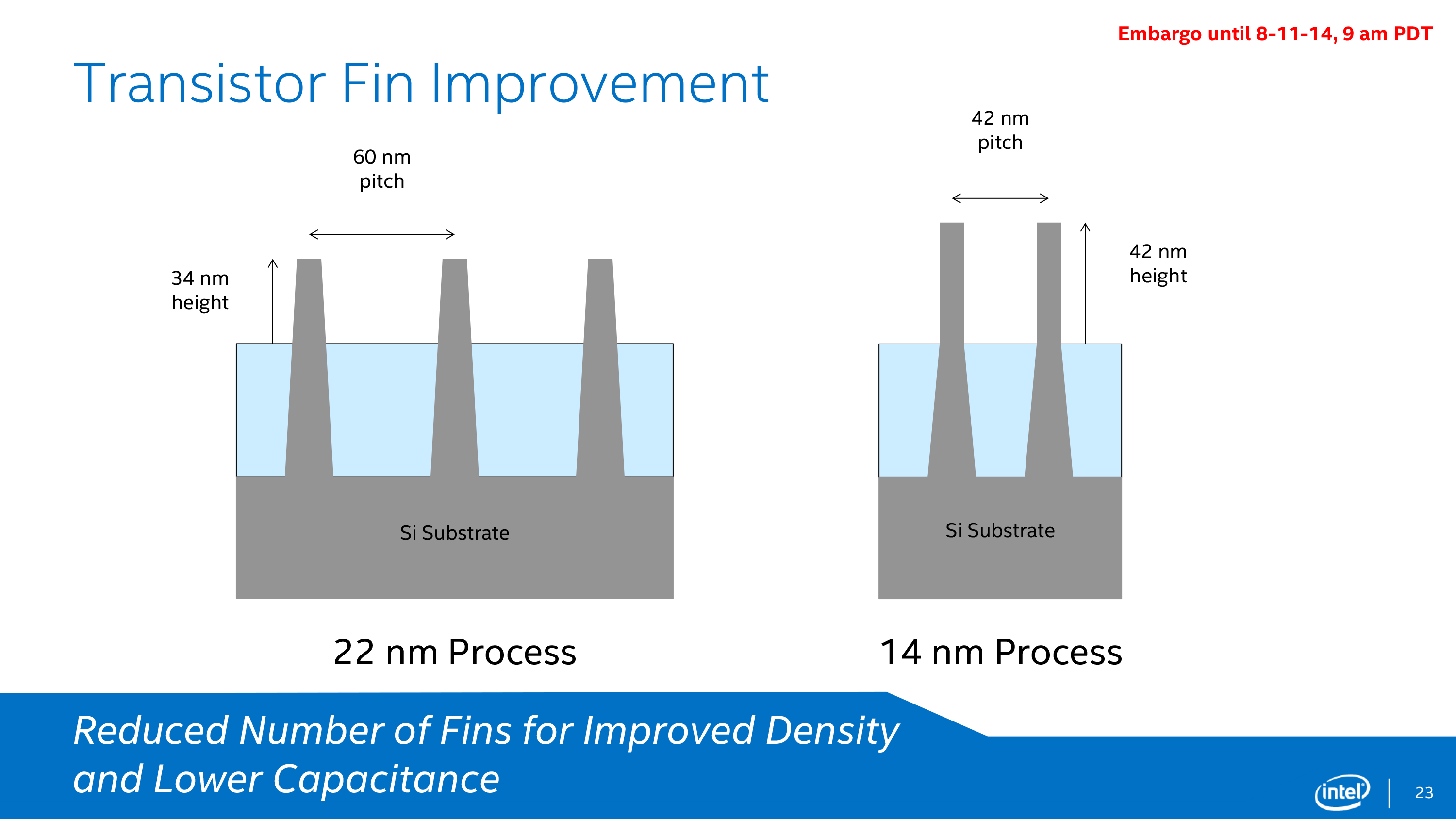
The main reason to going to 3d transistors/FinFETs is to have more control of the geometric layout of the gate channel and the electric field controlling the channel, thus reducing leakage current significantly.
To give you some idea. 22nm FinFET has much lower leakage than 28nm planar. I estimate that 14 nm FinFET is about the same as 28nm planar for logic but already worse for SRAM. 14nm FinFET is in any case worse then 22nm FinFET, because you cannot defeat physics.
At this point you need to think about clever designs, as for instance the big.little concept. Keep in mind Intel is already past the general FinFET/3-gate gain with respect to leakage.
Mind to enlighten me, how is this supposed to improve when going down to 10nm, even if you consider that you are using compound materials? I mean at some point you also need to reduce the thickness of the gate dielectric, where high-k materials are already used to extend Moores law.
I have to understand this. Does leakage go up in absolute terms when a node shrinks eg 28->20 planar or 22->14 finfet???

Sorry if my post was perceived as argument ad hominem. It was indented as advice.First things first, I'd appreciate it if you refrained from the use of ad hominem.
It is not question of budget nor a question of mediocre vs. good core it is a general principle. Strange that you seem to blindly believe Intel propaganda yet dismiss ARM propaganda. In any case objectively looking at the issue indicate that big.little seems like a reasonably good idea.If you don't have a big R&D budget, sure it might be cheaper to develop a mediocre big core and a mediocre little core, but SoCs like Apple's A series and Intel's Atom to me prove that a good core does not need a companion core.
I have to understand this. Does leakage go up in absolute terms when a node shrinks eg 28->20 planar or 22->14 finfet???
Well it is not all doom and gloom but a serious challenge. Power gating is quite aggressive already today. Props to Intel that they reduced the overwhelming amount of power states to C0, C1/C2 and C6 with Silvermont, which brings them closer to the ARM active-dormant-shutdown principle.Also, I have to say you are being a bit too doom and gloom about idle power. Power gating exists for a reason.
Windows doesn't support big little so it's kind of moot whether Intel likes it or not.
It was mainly about this sentence:Sorry if my post was perceived as argument ad hominem. It was indented as advice.
And while I'm at it, you repeated the same fallacy:Oh dear, please do not comment on topics, you are apparently no expert of.
I don't tell you to look at my avatar and interpolate my whole personality from there. Look at the content of my post.I have the feeling that someone with Intel sunglasses will not contribute objectively here.
Let's not argue about things we agree on, so I'm going to post what I'm disputing:Now back to the topic. You basically link random internet articles without contributing to the argument itself.
I contend this statement is wrong. The wrong assumption you made is that 14nm is the same process as 22nm, but ~2x denser. That is demonstrably false:I estimate that 14 nm FinFET is about the same as 28nm planar for logic but already worse for SRAM. 14nm FinFET is in any case worse then 22nm FinFET, because you cannot defeat physics.
The same happened with strained silicon, which went into its 6th generation at 14nm.We're confident this new transistor can be scaled further, and development is already well under way on our next-generation 32-nm transistors using an improved version of high- k plus metal gate technology.
I just added those as extra information, as I said. But it should be clear that leakage will go anywhere but down.90% of the linked information does not even apply to the question leakage at 22nm vs 14nm. Some of the articles discuss the move to high-k dielectrica few years back.
It isn't really propaganda because it's just used as technical information. You can't simply dismiss that information (Intel: "our 14nm has 2X lower leakage") and say your own "theory" is correct. I've given you a bunch of information from which it should be clear what will happen at 14nm, so it's up to you to provide more evidence for why I must believe you. I'm not going to believe you if you don't give me a reason to do so. But sure, I could be wrong. A definitive analysis from IDC would be helpful when Broadwell-K is released.The only thing, that was really applicable to the discussion, was a propaganda slide from Intel...nothing to add here.
I thought you would bring a real argument.
That is what I'd rather call propaganda (it's more information about the technology for the layman, but you get the point), which you were condemning 1 sentence ago.Interestingly if you go to
http://www.intel.com/content/www/us/en/silicon-innovations/standards-14nm-explained-video.html
they explicitly mention "reduction of active power"...no mention of leakage. Coincidence? I don't think so.
Where are your "objective" facts? Even besides the issue of any benefit it gives, the extra little cores will only give you an advantage when the CPU is not stressed anyway, so a downclocked CPU with power gated cores will already not consume much anyway, so the total amount of energy saved really won't be much if you have designed a big core with good power management.It is not question of budget nor a question of mediocre vs. good core it is a general principle. Strange that you seem to blindly believe Intel propaganda yet dismiss ARM propaganda. In any case objectively looking at the issue indicate that big.little seems like a reasonably good idea.
I think we concluded about 1 year ago that the power consumption of Silvermont is vastly superior than any planar ARM core; the performance per watt of Silvermont is unchallenged, so yes, it is not a mediocre core and it easily competes with Snapdragon 800.Even more surprising is, that you consider Atom a non mediocre SoC, yet it gets destroyed in performance by the competition at comparable power despite the big technology advantage.
It blows anything out of the water with regards to power consumption, but apparently only Intel has the tools to measure that. Silvermont is just a dual-issue architecture, so you shouldn't expect it too have a mind boggling IPC.One would assume that this thing is blowing anything out of the water that is still on planar, yet it does not. One would assume, that this thing is blowing anything out of the water, who uses fully synthesizable cores and not have full-custom parts, yet it does not.
'Cause I haven't seen any evidence that it has any meaningful benefit for big companies who can afford to build a good architecture from idle to high performance use cases.Anyway lets not get into discussion what is mediocre and what not,
Not sure though, that we ever see C6/shutdown in light use scenarios. That's where the big.little idea kicks in. Still don't know why witeken thinks this idea is stupid.
Yep. Capacitors (memory) do the same over time. As does flash memory.The person in following video predicting what Intel's 14nm transistor would look like, in 2012, within half a minute in the video.
https://www.youtube.com/watch?v=lL5A4DblL3E
It blows anything out of the water with regards to power consumption, but apparently only Intel has the tools to measure that.
I'm tired of busting this myth, but the CPU is not the biggest contributor to platform power consumption in mainstream use cases. Certainly not when the screen is 13.3" and has 6MP to feed.On BW size cpu the burden of decoding is ofcource of far less importance than BT - and perhaps relatively insignificant.
But the problem is, when we talk BW size we have the leaking challenge as shown by the battery life problems. If they are not going to improve much with new nodes - clearly there is a challenge. We have a single product, so its to early to know for sure, but as of now, it clearly points to a challenge and problem.
I'm tired of busting this myth, but the CPU is not the biggest contributor to platform power consumption in mainstream use cases.
I am looking forward to the first 18 tdp (?) parts for the ultrabooks. When are they due? And what can we expect from cpu and gpu perf?
Intel should have had some "ultra book" standard for Core M and limited it to 1080p.
A Super High Res is neat and all but 90% of the people purchasing a laptop of the size Core M is supposed to enter couldn't care less about "QHD" screens.

No one was claiming, that the CPU is the biggest contributor, when the screen is on. However it is still a contributor and just cannot be neglected. In particular since leakage is increasing in absolute terms.I'm tired of busting this myth, but the CPU is not the biggest contributor to platform power consumption in mainstream use cases. Certainly not when the screen is 13.3" and has 6MP to feed.
Is Core M the only broadwell variant available for 2014?
I hope they will be launched at CES, but someone who has paid closer attention to the roadmap might correct me (it should be somewhere in Q1).
Citation needed.In particular since leakage is increasing in absolute terms.
Due to the fact it is OLED this would be nice but Windows 10 better do resolution correctly or you are in a world of hurt.I Could use a new Samsung 13.3 ultrabook with oled 4k
And then hope win10 is going to be a new win7/xp. (Yes i want the 270ppi if its pentile on oled 😉)
You still do not get it. This fact comes from laws of (quantum) physics.Citation needed.